I think this is a heroic effort and really interesting. The flux gate shares a lot with an LVDT and I was wondering if an LVDT conditioning chip like this: http://www.analog.com/media/en/technical-documentation/data-sheets/AD598.pdf could simplify the project? They have a lot of the key pieces integrated.
The excitation part of the conditioner could be reused (except that here the frequency is 50KHz), but the signal processing section is quite different.
In addition, it has to work at twice the base frequency.
Maybe possible with an older IC, having lots of pins and outside components.
There might be other specialized functions/chips better suited to task, but some lateral thinking would be necessary to identify them
In addition, it has to work at twice the base frequency.
Maybe possible with an older IC, having lots of pins and outside components.
There might be other specialized functions/chips better suited to task, but some lateral thinking would be necessary to identify them
You are right: I have to update the exciter schematic, and to write an alignment procedure.Hi Elvee,
Any updates to the documentation for this project?
I have been rather busy with other things, and I have somewhat neglected this one. It's on my to do's list...
You are right: I have to update the exciter schematic, and to write an alignment procedure.
I have been rather busy with other things, and I have somewhat neglected this one. It's on my to do's list...
I totally understand. My granddaughter just arrived. She's 4 1/2 going on thirteen so I am occupied for a while as well!
")
Corrupt file
The attached file Fluxgate.zip appears to be corrupt. Could you upload again, or send a copy directly to me?
dgminala at mediacombb dot net
Many thanks!
Looks like my answer has been ejected....
Bis repetita, etc..
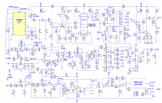
I post the entire (raw) folder, including purely graphic items, working subsections, etc.
Note that all may not be up to date, because final refinements were carried out at a phy level, not in sim.
R65 is a good candidate for a larger size: under normal circumstances, 0.25W is sufficient but in case overloads happen, 0.5W or 1W is preferable
The attached file Fluxgate.zip appears to be corrupt.
Could you upload again, or send a copy directly to me?dgminala at mediacombb dot net
Many thanks!
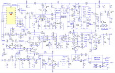
Here is the revised schematic, and a tentative alignment procedure.
The revisions concern mainly the addition of two resistors in the emitters of Q1/Q2, and the splitting of R10.
The resistors for Q1 and Q2 are mandatory, the other mod is just recommended, but is somewhat beneficial too.
If you find difficulties applying the alignment procedure, let me know, I'll try to revise it.
Attachments
Hi Elvee,
Demian remembered this thread for me. I have three complete 428B units that I'm running. I love them too. But your project would allow me to keep a modern version on the bench instead of shelves in the back. I had bought the last one as spare parts, but then noticed someone selling probes. I bought one to complete that unit.
I don't know when I'll have time to design a PCB for this project, but ultimately I'd very much like to have a pair of these meters in one box so I can monitor two currents at once.
Thanks so much for documenting your project and giving me a place to start. Your work is inspired, and many share your love for this instrument.
-Chris
Hi Sander,
I found a spare probe on Ebay for a meter I got without one. Just keep you eyes peeled for one as they do crop up from time to time. I think you can also post a wanted ad. Finally, sometimes you can get the entire meter and probe for what a probe would cost. Your existing meter then becomes a parts unit as the meter needs to be calibrated with the probe you are using. You can't just plug one in and go.
Good luck!
-Chris
Hello Elvee
I'm looking for a probe for my HP428, mine is broken
Maybe you want to sell one, and send to Holland?
Sander
Sorry Sander, but I prefer to hold on to them, precisely as a plan B in case of breakage.
Your best option is to follow Chris's advice
Hello everybody. I didn't post anything so far on this forum but i take a peek now and then.
Couple of years back i saw this topic and bought HP probe that i hope is working, i don't have anywhere to test it. I checked it with DMM and both coils are ok, but ofc i won't be for sure until i build this instrument and plug in probe.
Now let's get back on topic. Since i saw this schematic i had a plan to make a PCB to make things easier for those that wanna build this.
I started to draw schematic in EAGLE but i have few questions about it cause some elements are not marked. I tried to compare schematics to pictures on first page and made some conclusions but this is electronics and if you are not sure in something better to ask then to watch white smoke after you turn on device.
So let's start with questions. Looking at schematic from post 29 i got few questions. OPamps are not marked and looking at pictures of completed device i made some assumptions. U3-LF347, U4-TL074, U7-TL072,is that correct?
Next thing that is puzzling me is cd4060 400Hz output that goes to RMS to DC converter, where that thing goes? I know you said true RMS to DC converter you used is proprietary circuit and we can use some other but i checked some true RMS to DC designs and didn't saw input for some extra signal(like yours 400Hz output from 4060).
Last thing is related to U5-CD4053 and U2D-CD4069 output which goes to some pin on 4053 but i coudn't figure out where it goes.
I think that would be it for now, when i complete schematic i will start with layout of PCB. That will take some time cause this is great project that deserves really good layout.
Once again thank you Elvee for your effort designing this and i hope that once i finish layout somebody will have a good use of it.
Best regards,
Davor
If you test the inductances of the coils and find them similar, and if the probe is in a good mechanical condition, chances are it is OKHello everybody. I didn't post anything so far on this forum but i take a peek now and then.
Couple of years back i saw this topic and bought HP probe that i hope is working, i don't have anywhere to test it. I checked it with DMM and both coils are ok, but ofc i won't be for sure until i build this instrument and plug in probe.
So let's start with questions. Looking at schematic from post 29 i got few questions. OPamps are not marked and looking at pictures of completed device i made some assumptions. U3-LF347, U4-TL074, U7-TL072,is that correct?
They can all be of the TLOxx series, or the LFxxx series, or any similar biFET amps.
Note that many non-FET amps will also work, if they have similar or superior characteristics (without excess though).
You are free to arrange the operators as you find convenient, or you could use duals everywhere if you find it more convenient, etc.
That's precisely because it is my proprietary design....Next thing that is puzzling me is cd4060 400Hz output that goes to RMS to DC converter, where that thing goes? I know you said true RMS to DC converter you used is proprietary circuit and we can use some other but i checked some true RMS to DC designs and didn't saw input for some extra signal(like yours 400Hz output from 4060).
In your case, you can omit the components around U2E
It goes to the two control inputs of the switches in question A and B: 11 and 10.Last thing is related to U5-CD4053 and U2D-CD4069 output which goes to some pin on 4053 but i coudn't figure out where it goes.
Here again, your are free to arrange the operators as you prefer
Yes, and keep in mind that one the difficult aspects of the projects is the inductive components.I think that would be it for now, when i complete schematic i will start with layout of PCB. That will take some time cause this is great project that deserves really good layout.
If you have little or no experience with this type of component, it would be imprudent to embark on such a project.
Also note that the absolute value of the 6.5MHz is unimportant: only a half-decent stability is sufficient (a good LC oscillator would also work).
A deviation of +/-2% on the absolute value is acceptable.
I am sure many people willOnce again thank you Elvee for your effort designing this and i hope that once i finish layout somebody will have a good use of it.
- Home
- Design & Build
- Equipment & Tools
- Modernized HP428 clone