Another option for MCLKI would be a self-contained oscillator module. Then you could drive the '1701 and '5102 with the same line.
After careful re-re-reading of Using The Oscillator, pg 18 of the '1701 PDF, it does appear that only fundamental mode crystals in the 12MHz range are supported. Since crystals in the 24MHz range are generally 3rd-overtone (unless of course there is some new technology that I'm unaware of ..), what you have probably won't work.
Try not to worry about the mistakes -- we've all made 'em. I think you've done great getting this far! It's a 52 page PDF, after all, and not always *the best ever* technical writing.
Good take on the PLL_MODE0/1 options -- might be a good candidate for jumpers on the next board iteration -- but again, not what would be considered a 'mistake'. Part of the fun/challenge of this generation of parts, is sorting out what they can do reasonably, without getting seduced by what maximum-magic it might be capable of.
Thanks for posting, Neil Davis. I'll want to spend some time studying those links but at a glance or two, it looks like great stuff. Thanks again for sharing it.
It's one of my favorite things about this forum -- setting out to spend a few minutes just checking up on a thing or two, then realizing hours later that I just *got learned up* on a bunch of new stuff! (New to me, anyway ..)
Regards
After careful re-re-reading of Using The Oscillator, pg 18 of the '1701 PDF, it does appear that only fundamental mode crystals in the 12MHz range are supported.
Since crystals in the 24MHz range are generally 3rd-overtone (unless of course there is some new technology that I'm unaware of ..), what you have probably won't work.Try not to worry about the mistakes -- we've all made 'em. I think you've done great getting this far! It's a 52 page PDF, after all, and not always *the best ever* technical writing.
Good take on the PLL_MODE0/1 options -- might be a good candidate for jumpers on the next board iteration -- but again, not what would be considered a 'mistake'.
Part of the fun/challenge of this generation of parts, is sorting out what they can do reasonably, without getting seduced by what maximum-magic it might be capable of.Thanks for posting, Neil Davis. I'll want to spend some time studying those links but at a glance or two, it looks like great stuff. Thanks again for sharing it.
It's one of my favorite things about this forum -- setting out to spend a few minutes just checking up on a thing or two, then realizing hours later that I just *got learned up* on a bunch of new stuff! (New to me, anyway ..)
Regards
Last edited:
Member
Joined 2018
Hi Baldin-San,
Well, I know 2SB1302 is too big to fit this spec. I choose this following 2 reasons. At first, It's easy to get "Akihabara" here in Japan. The second reason belongs to my prototype board. It used another SOT23 package Tr for this part but it seems need to add heat sink or something like that, so I changed it without deeply through....
Also the HC-49S crystal is easy to get at shops here, and I thought I might need to change crystal frequency for synchronizing with 48kHz/44kHz application. I used pin-socket for my prototype version. Current design inheriting those old situations. If I could have a chance to next generation board design, I will choose 24.576MHz NDK TCXO instead of crystal.
Updated Design and Layout
Ok, have made the decision to make an updated PCB correcting the mistakes. See PDF (GND layer not shown for PCB to make it easier to look at).
Changes made:
- Q1 for VDrive changed for a DXT5401 SOT89 to allow for a little more dissipation. Also made two small "heat sink" areas on top side.
- Dropped the Mute resistors to 12V ... so now only connection to the ADAU1701 port. Assuming that the internal pop elimination in the PCM5102 works at power up and down. So the soft mute only to be invoked by the DSP. Will have to find out how to control this at start up of the DSP. Question, can you rely on the output being either high or low, always at start up / Initialization of ADAU1701??
- Changed Xtal to 12.288 MHz (X322512288MOB4SC)
- Changed PLL Mode pins to match Xtal for 48kHz operation
- Changed R13 to 100 ohm and connected to MCLK pin 31 on ADAU1701 OSCO
- Added a LED to +12V just to see that there is power on the circuit
- R9, R11, R12 .... not moved ... not really room to get them closer to ADAU1701.
- Changed the 2 pin Terminal block for a smaller one pitch 3.5 mm
Question, C29, C30, do these have to be C0G? .... not in JCLPCBs DB, so using X7R
CyperPit, saw you are using beads around PCM5401 .... is this because you have seen a real need, or just anticipating digital noise in general?
.... Hope I'm getting it right this time
Attachments
Last edited:
You might still need to select a Q1 with higher DC current gain -- the Diodes Inc by that p/n shows it as only 60 @ 10mA, and it's likely to be lower still at the specified max of 60mA. It may measure perfectly fine at initial checkout, then sag badly yielding erratic performance as the processing load on the *Core* rises. The spec PDF says to select for a minimum beta of 100; I'd encourage that. The good news is, now that you've increased the footprint to an SOT-89, you have more options. Power dissipation won't factor into it because the voltage across it is only 1,5V -- that's only 90mW at 60mA. Maybe check for one of the Zetex p/n's from Diodes Inc; they're more expensive, but higher gain than most.
X7R may work OK for C29 and C30. But since they're in the PLL loop filter, leakage and +/-10 to 30% capacitance change over temperature and voltage could cause an intermittent and hard-to-track-down problem. A better option might be to have JCLPCB leave those unfitted, then mount a couple C0G's or NPO's yourself. At the very least I'd plan to replace the X7R's at the earliest opportunity.
Cheers
Would also recommend *bleeder* resistors (or whatever the common name is for them) on the 'Outside World' side of C28 (InL), C31 (InR), C8 (FLTOut0), and C12 (FLTOut1). For those times that the capacitor has a charge before connector mating, or the other equipment has its own blocking capacitor.
Thanks Rick, for the review. Very good points, that I'll follow. Will try to fir some 0805 COG for the PLL and fit them myself, and will find a more suitable transistor with higher Hfe ... actually thought about that but never got around to it.
Also the bleeder resistor (think it is the right/common term for a resistor to discharge a cap) is a good idea for sure.
Will make an update to schematics and PCB in the coming days ... when work allows
Cheers Baldin
Also the bleeder resistor (think it is the right/common term for a resistor to discharge a cap) is a good idea for sure.
Will make an update to schematics and PCB in the coming days ... when work allows
Cheers Baldin
Member
Joined 2018
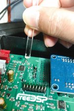
Bead is working
Hi Baldin-San,
About Bead:
I checked with bypassing Beads FB1/FB2/FB3.
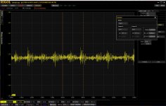
I can hear increasing remain noise in high-frequency range when I shorting the FB1/FB3. ( Please refer the attached picture)
I could not heard the difference when I shorting the FB2.
The difference is too small to show in the numerical difference with my measuring equipment. (Except ears)
About New Schematic:
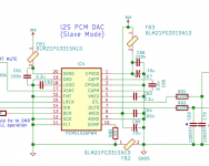
If you want to add solid-state muting to your ADAU1701 embedded DAC outputs, you can use PCM5102A pin5 for the negative bias voltage source for releasing muting transistors.
The other part comment was covered with Rick-San's comments.
Hi Baldin-San,
About Bead:
I checked with bypassing Beads FB1/FB2/FB3.
I can hear increasing remain noise in high-frequency range when I shorting the FB1/FB3. ( Please refer the attached picture)
I could not heard the difference when I shorting the FB2.
The difference is too small to show in the numerical difference with my measuring equipment. (Except ears
)About New Schematic:
If you want to add solid-state muting to your ADAU1701 embedded DAC outputs, you can use PCM5102A pin5 for the negative bias voltage source for releasing muting transistors.
The other part comment was covered with Rick-San's comments.
Attachments
Thanks CyperPit,
Ok think I'll make room for a few beads .... the cost is almost nothing
... why did you not include a bead for AVDD?
Good idea to use pin5 as negative bias for muting transistors .... will maybe come back to this. On the other hand for now I'm only planning to use the 2 outputs from PCM5102 .... but in a next design ...
Ok think I'll make room for a few beads
.... the cost is almost nothing ... why did you not include a bead for AVDD?
Good idea to use pin5 as negative bias for muting transistors .... will maybe come back to this. On the other hand for now I'm only planning to use the 2 outputs from PCM5102 .... but in a next design ...
Last edited:
Member
Joined 2018
Why FB2?
Hi Baldin-San,
It's out of stock of my parts box...
I will replace and compare the difference later.
Hi Baldin-San,
The reason?why did you not include a bead for AVDD?
It's out of stock of my parts box...
I will replace and compare the difference later.
Member
Joined 2018
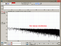
The difference belog to Bead FB1
Hi Baldin-San,
I checked to know the beads insertion difference around PCM5102A.
The difference was FB1 > FB2 >> FB3(very small)
Attached animation GIF shows bypassing FB1 or FB1 Working in my FreeDSP Classic SMD A/B plus II board (40dB Boosted to see the remain noise)
Hi Baldin-San,
I checked to know the beads insertion difference around PCM5102A.
The difference was FB1 > FB2 >> FB3(very small)
Attached animation GIF shows bypassing FB1 or FB1 Working in my FreeDSP Classic SMD A/B plus II board (40dB Boosted to see the remain noise)
Attachments
Last edited:

Ready for ordering new PCBs ... I think
Chose 3 beads for the PCM5102:
PCB Prototype & PCB Fabrication Manufacturer - JLCPCB
Each for CPVDD, AVDD and DVDD.
Just chose one of the basic components they have to save a few USD, therefore the 0805 casing.
600 ohm at 100MHz
Chose 3 beads for the PCM5102:
PCB Prototype & PCB Fabrication Manufacturer - JLCPCB
Each for CPVDD, AVDD and DVDD.
Just chose one of the basic components they have to save a few USD, therefore the 0805 casing.
600 ohm at 100MHz
Attachments
Still think your WB line is going to react too slowly to provide the desired function.
You could connect R38 to the Collector of a PNP whose B-E junction either replaces D1 or is in series with it. Choose a large area part, say a MMBT4403, and a fairly low-value resistor, B-E to share the supply current and hasten turn-off. Then adding a 'normal value', maybe 4k7, B-E on Q2 would improve its turn-off attitude.
Otherwise, it's a long ways down from 11.4V, to the few hundred mV Q2 needs to stay on. By that time all the regulators have dropped out of reg, the Low Voltage detects have triggered, and there's no juice left for the flash to write with anyway.
Just my two bits ..
Cheers
Last edited:
Hey Rick
You are right about the WB signal being too slow if implemented as suggested. I had simply copied the part from the schematics for the EVAL board.
Two options I think: either use a dedicated voltage monitoring devices like the ADM812 or TCM809TENB713, or making a detection on the input side of the regulator, set for something lik 4.5V. More or less same circuit as before, but with a Zener on the basis to detect the 4.5V.
On the other hand I do not really foresee the use of the Write Back option as I'm using real potentiometers for the input of voltages, and not e.g. a rotary decoder, where one might want to use the settings for e.g. volume for next "session".
So I will simply omit this part and let WB be disconnected.
Have updated around the voltage input, inserting a 0R resistor, which can be omitted at first trail just to make sure the regulator is indeed putting out 3.3V.
And have changed the transistor for DVDD to a Zetex type (ZX5T3ZTA) with much higher Hfe (flat up to 1A). A bit overkill but it was the best suited I could find at JLCPCB (can be omitted from JLCPCB and I could chose another type and solder myself).
Think I'm ready for sending to production .... unless you see other faults
Attachments
New PCB first trial ....
Got the PCB back from manufactory.
Somehow had forgotten to get the transistor for DVDD mounted, so had to use a BC556B (with a bit of leb bending) in stead.
The line reg gives the 3.3V as it should, but I only measure 0.1V at DVDD!
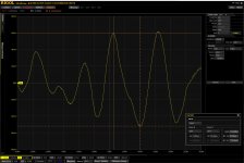
The OSC out does no really give any meaning full ... see picture.
The 3.3V regulator gets a bit hot, so some current is for sure running (also 16V in, so quite a drop).
Hmmm what to try next?
Got the PCB back from manufactory.
Somehow had forgotten to get the transistor for DVDD mounted, so had to use a BC556B (with a bit of leb bending) in stead.
The line reg gives the 3.3V as it should, but I only measure 0.1V at DVDD!
The OSC out does no really give any meaning full ... see picture.
The 3.3V regulator gets a bit hot, so some current is for sure running (also 16V in, so quite a drop).
Hmmm what to try next?
Attachments
- Home
- Source & Line
- Digital Line Level
- ADAU1701 based DSP for sub or 2 way