The LM317 resistive divider values need work. You may also want to include the 1N4002's mentioned in the data sheet, esp since you have somewhat larger capacitors.
The inputs and DAC_OUT2 and DAC_OUT3 need a large value resistor to ground -- otherwise the MUSE caps will have no incentive to charge. Also, polarized electrolytics would be fine in this use (at least as OK as any electrolytic) since you have a consistent polarizing voltage.
Lots of nice work.

The inputs and DAC_OUT2 and DAC_OUT3 need a large value resistor to ground -- otherwise the MUSE caps will have no incentive to charge. Also, polarized electrolytics would be fine in this use (at least as OK as any electrolytic) since you have a consistent polarizing voltage.
Lots of nice work.
.. and .. a couple other things -- but Remember, this is your project! Make it the way YOU want 😉
- the MMBT5401 is a relatively high voltage type - it may not have the specified hFE 100 at such a low Vce; it would probably worth the extra cost of a Zetex part since the 1.5V Vce can challenge even 40 and 60V parts - and it would be an awful waste of half a weekend if the 1.8V was flopping around in some code-execution-dependent manner
- consider 74LVC1G04 or -14's to drive the LED's - naked outputs only provide 2 mA
- a 10nF or so cap to filter each 10k pot wiper might be good, and
--- full scale for that ADC is 3.0V -- a 750 ohm or 1k in series to the 3.3V would keep the top 1/8 or so of the rotation from being wasted (that is 'giving no control change')
- I think your WB circuit will be too slow - another good job for an 74LVC1G14, maybe with a 3k3 pull-down on its input, then 680 ohm and 8V zener to the collector of a PN/MMBT2907 whose base-emitter junction replaces D1
- most microcontrollers hate slow reset signals - consider buffering (LVC1G14 ?); I haven't found anything in the data PDF about this one tolerating a 100 microsecond time constant; also, you may want to include a push-button so you can force a reset without removing power
Glad you're back on it -- this is a neat project.
Cheers
Last edited:
Not working ... any ideas????
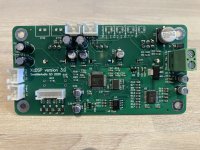
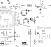
Have progressed somewhat with my first ADAU1701 board.
Have gotten the PCB made and populated at JLCPCB, at least for most of the SMD components.
I opted to go for a PCM5102 as DAC to make sure I have some pop free outputs.
See PDF for details.
Have mounted rest of the components, and tried to power up, but I only get 1V DC at the output of the LM317 ?!?!?!?
Scratching my head. What can be wrong?
I have 16 V dc in, so more than enough for the regulator to work.
Over current protection on the LM317 due to fault somewhere else??
Have tried to change the LM317 to see if this was what was wrong.
Have checked the resistors .. correct values.
I know it is no conclusion to anything, but measured the resistance from GND to +3V3 and this is 25 ohm.
I have two boards made from JLCPCB, and they measure the same resistance.
Also measured this resistance while I had the LM317 not mounted, and it's the same. ..... not sure what I would expect to see though!
See pdf for details
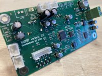
Attachments
Ahhhhh found an erroer :| pin 1 AGND is connected to 3V3 and pin 48 AVDD is connected to GND ... should of course have been the other way around .... better review some would say 😉
Maybe I can lift the pins and connect to right pad with a very thin wire .... but not easy
Maybe I can lift the pins and connect to right pad with a very thin wire .... but not easy
Wonder if the chip has been damaged?
Have lifted the pins, but now I need to re-connect .... not so easy 😉
And thanks for helping and spotting the error 🙂
Have lifted the pins, but now I need to re-connect .... not so easy 😉
And thanks for helping and spotting the error 🙂
Member
Joined 2018
In your schematic, aren't the PLL mode pins set up for 384 x Fs? That would require an 18.432MHz crystal for the "conventional" 48K sampling rate.
ooops--nevermind. Looks like that got changed in a later version of the schematic.
ooops--nevermind. Looks like that got changed in a later version of the schematic.
Last edited:
Good points Cyberpit and Niel Davis. Thanks.
See Schematics in post #23
PLL_Mode_0 = 1
PLL_Mode_1 = 0
=> 384 x fs
Xtal = 24.576MHz => fs = 60 kHz ....... that is going to be a bit unconventional ... but I guess it will still work ok.
Changing to 12.288 MHz would give 32 kHz ... more conventional 😉 .... But I do not have a Xtal that will fit, so will have to try it out.
Anyway don't know yet if it works at all. I had a good friend at work do the soldering to switch the two pins, a person how is used to work with even smaller components and wire.
I'll try to hook the PCB up today
Now the AVDD is working at 3V3, and DVDD is 1V8.
But MCLKI is nothing but noise ... see picture.
I'm using an AT cut fundamental Xtal from JLCPCB
https://datasheet.lcsc.com/szlcsc/Yangxing-Tech-X503224576MSB2GI_C112568.pdf
100 ohm series resistor and 2 x 22 pF
But MCLKI is nothing but noise ... see picture.
I'm using an AT cut fundamental Xtal from JLCPCB
https://datasheet.lcsc.com/szlcsc/Yangxing-Tech-X503224576MSB2GI_C112568.pdf
100 ohm series resistor and 2 x 22 pF
Attachments
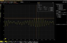
Doesn't look like noise to me -- it's trying to oscillate.😉
Maybe try probing OSCO (pin31), instead of MCLKI (pin 32).
Do the amplitude dips happen to coincide with dips in the 1,8V regulator (pin 13)?
Cheers
Maybe try probing OSCO (pin31), instead of MCLKI (pin 32).
Do the amplitude dips happen to coincide with dips in the 1,8V regulator (pin 13)?
Cheers
And, not to be a Debbie Downer, but the odds of the '1701 still behaving perfectly after the pin 1 / 48 connection swap are not really great.😱
Sorry
Sorry
The MCLKI for the '5102 should come from the OSCO side of R23 -- it can not come from the return side of the crystal.
You may need to cut the trace from C35 to R13 at both ends, to eliminate the stray capacitance (ground plane on the other side, for starters) and EMI pickup. Then fit a jumper from R13 to the pin 31-side of R23; or install a buffer as recommended in the '1701 PDF -- maybe a 74LVC1G04 or -G14.
Oh, and, if you do re-do the board, you could eliminate 4 feed-throughs in the mute line: Swap R8 / C15 and bump them and R7, C10 half a space farther away from R13. Both Mute and Clk can come in around the 'south' side of the oscillator section.
The row of 22R resistors belong closer to the outputs driving them. Their job is softening the edges a bit, giving less bounce at the receiver.
R7 trying to pull Mute up to 12V is probably not a good idea, either. Besides forward-biasing substrate diodes, the Mute signal will still be well above its threshold (somewhere between 3,3V and ground) when the regulator drops out of regulation.
It may also be necessary to remove the ground plane under the oscillator traces, or possibly just reduce the 22pF's.
Cheers
Last edited:
Member
Joined 2018
The crystal frequency for ADAU1701 limitation FAQ.
ADAU1701 with 24.576MHz crystal? - Q&A - SigmaDSP Processors and SigmaStudio Development Tool - EngineerZone
You can connect OSCO to PCM5102A like this way, but you can't use 192kHz fs with 12.288MHz MCLK. Need to invoke PLL of PCM5102.
I faced this limitation on designing FreeDSP Classic SMD A/B plus ][.
Regards,
Attachments
Last edited:
Hi Rick and CyperPit
Thanks a lot for the input. Highly appreciated.
Year, think it is highly unlikely the the ADAU1701 has survived the pin swap.
Ok also seem I have been way to fast with this design 😉 ...... and a total newbie in this field on top 🙂
Well, we are here to learn and have fun.
I'll work some more at it today. Think I need to make a new PCB ... too many mistakes to be sorted starting with the Xtal. I actually found another Xtal on 12.288 MHz, but is has a different pad layout, and will not be easy to mount. ... need to get myself a microscope 😉
Also as I see it I would need to change PLL_Mode1 to 3V3 and PLL_Moce0 to GND, to obtain a fsx256 giving a sample rate of 48 kHz. For any design soon I do not need 192 kHz and 48 kHz will be just fine.
I had really hoped to be able to test the design working around the mistakes. I fear a little spinning a new PCB, with possible more errors! Not so much the money, but the time to get it manufactured 😉
Will look at you suggestion Rick, and incorporate in new schematics and PCB.
PS. @CyperPit .. see you are using a 1W 2SB1302 transistor for providing the DVDD, is this really needed? ..... I was using a MMBT5401 (350mW) ... for size!
PPS: See most using rather big sized Xtals ... any thoughts on that? ... I was planning on using small SMD types
PPPS: @CyperPit, had not seen you FreeDSP Classic SMD A/B plus II design ... cool ... will compare and learn 😉
Last edited:
If you are considering an update to the PCB, you might want to consider using the "modules on a motherboard" approach. I made a lot of ADAU1701 circuits for the designs at Audiodevelopers, but once the ADAU1701 learning module became available for less than $20, it didn't make sense anymore to use my own circuitry. I couldn't buy the parts for less than that, and assembly required several beers, adding to the cost. The first run of boards is described in article 6 and the newer approach is shown in article 16.
I haven't been putting a lot of effort into this recently, but with winter on the way ("software season") I'll be refactoring the code into libraries and making it available to others. What I have is a nice high-level interface that allows control of the high-level DSP functions from a cell phone app--it's the only way to go, IMO.
I haven't been putting a lot of effort into this recently, but with winter on the way ("software season") I'll be refactoring the code into libraries and making it available to others. What I have is a nice high-level interface that allows control of the high-level DSP functions from a cell phone app--it's the only way to go, IMO.
Hi Neil
You are probably right, and it would be a ot faster road to success.
But I like the challenge, and at JLCPBC 20USD actually goes a long way, for producing PCB and populating with most SMD components.
This first DSP is a bit of a trial version, and should fit into a Soundbox, and will also be suitable for a subwoofer.
Will probably take the design to the next step for a 3 way configuration, maybe going for more powerfull DSPs and better ADC / DAC ........ but I think this is probably somewhat far into the future with all the mistakes I'm making 🙂 🙂 🙂
- Home
- Source & Line
- Digital Line Level
- ADAU1701 based DSP for sub or 2 way