Maybe, I've missed something, but the schematics don't appear to show why this would be considered Germany's ultimate DAC. Rather, seeming quite average. I can't read the German reviews, so, perhaps you can clarify?
Ken, this is even the MOST ultimate DAC 😀 (Whatever that grammatically means)
German magazines do not test gear like this, as it is not a true branded production piece of equipment
well you are right more mediocre. Probably the MOST peculiar DAC, that would be more like it
I still do not get it why OP is not spending his time on building a good DAC and just stop with this strange and outdated thing.
But that is just my 2 cents - it is a hobby and I am not going to tell people what to build of course
Attachments

Last edited:
Are You sure that direction of diodes are right? I think that they have diferent directions at + and - branches? And they are also diferent at pictures. Connections with 2W resistors?I have never seen before this approach of voltage regulation - it confuses me. Basically, there are two series regulators connected in series. The second series regulator generating a stabilized voltage that is below the desired values - go to the attached circuit diagram.
The desired values are obtained by connecting resistors of a certain value in parallel to the second voltage regulator, which are adjusted to the individual power consumption both of the DAC and high pass filter/buffer modules.
The marked 270R resistors are overheated but not defective.
The series diodes prevent voltage from flowing back into the output of the second regulator, unfortunately not in the first regulator because of the resistors connected in parallel to the second regulators (please note - behind the output of the second regulator stages are connected very large capacities of approximately 400.000µF/each rail - outside of the capacitors are nothing to read).
I want to create a parallel regulator resp. shunt regulator concept.
What needs to be considered here ?
Thanks for an advice and calling the appropriate topics here on diyaudio.
.
BTW I think that You should change this regulator. 🙁
I'd 1st measure the current draw and then calculate the total power dissipation in each rail. I'd regard these bypass resistors as a crutch as they surely affect the PSU's performance in terms of regulation and output noise. Maybe you can try to mount all four LM's at a bigger sink and toss these resistors? Or to increase the series resistors at the LM's inputs?
Best regards!
Best regards!
The designer of this DAC (Michael Pavischitz) was also the designer and producer of the Dynaudio Arbiter power and pre amps. These were indeed praised by German and also international Hifi critics as "Ultimate" or "Landmark" amps.
From what I can see in the schematics, I doubt that his DAC lives up to this reputation of its designer (Not even close).
For me clearly the PSU destroyed the DAC chip, after it was certainly stressed a few hundred times during power on and off, by these 0.5mOhms ESR CAP banks.
If there is a high leakage or loss in capacitance in these huge caps, there is the chance, that one rail doesn't come up at all or faster up or down than the other. These are things, a PCM1702 doesn't like at all. The leakage in the huge caps may also have destroyed the parallel resistors on the LM317/337.
IMO this design was made under drugs 😀 It may have worked quite well as a prototype, but it is not robust in any way.
I would check the cap bank leakage and cap values and recap them if necessary and recommend the user to sell this unit and buy a Parasound D/AC-1100, which has a very similar architecture/sound potential and the better DAC chips (PCM63) and filter (PMD100) as well.
Or tell him to NEVER SWITCH THIS UNIT OFF after repair. 😀
Any radical change drops the resale value of this DAC to almost Zero.
Last edited:
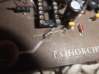
From an interview with Michael Pavischitz:
"Im Grunde genommen kann man sagen, daß diese Wandler (Steps 1 und Steps 2) technologisch eine Weiterentwicklung (Anm.: Des Arbiters) darstellen.
Sie sind in vieler Hinsicht absolut ultimativ. Sie haben zum Beispiel ein Netzteil, das so aufwendig gemacht ist, daß es durch Batterieversorgung nicht mehr zu verbessern ist. Wir ersetzen die Batterie quasi durch extreme Kapazitäten."
So he tells us, that the power supply of the STEPS DACs is a "technological improvement" over the Dynaudio Arbiter amp. In this aspect the STEPS DACs are "absolutely ultimate". 😀 The PSU is so good, it could be not bettered even by batteries.
As we can see, he is easily able to compare apples with oranges (build on the reputation of the amps) and shows that the "double superlative" language about the DAC comes from the designer himself, which on the other hand is a good sign of healthy self conciousness, which we all know is always a guaranty of a well done "job" . 😉
. 😉
To summarize the response of this forum so far: We have here an overall mediocre DAC with a "double superlative" PSU, which grilled the highly selected mediocre DAC chip first and afterwards itself ...
I would repair it to as-new condition and sell it, as fast as I can.
Can you tell us, what your friend paid for it ?
Btw.: MSRP: 37500 DM (~20000 EUR, ~22000 USD).
"Im Grunde genommen kann man sagen, daß diese Wandler (Steps 1 und Steps 2) technologisch eine Weiterentwicklung (Anm.: Des Arbiters) darstellen.
Sie sind in vieler Hinsicht absolut ultimativ. Sie haben zum Beispiel ein Netzteil, das so aufwendig gemacht ist, daß es durch Batterieversorgung nicht mehr zu verbessern ist. Wir ersetzen die Batterie quasi durch extreme Kapazitäten."
So he tells us, that the power supply of the STEPS DACs is a "technological improvement" over the Dynaudio Arbiter amp. In this aspect the STEPS DACs are "absolutely ultimate". 😀 The PSU is so good, it could be not bettered even by batteries.
As we can see, he is easily able to compare apples with oranges (build on the reputation of the amps) and shows that the "double superlative" language about the DAC comes from the designer himself, which on the other hand is a good sign of healthy self conciousness, which we all know is always a guaranty of a well done "job"
. 😉 To summarize the response of this forum so far: We have here an overall mediocre DAC with a "double superlative" PSU, which grilled the highly selected mediocre DAC chip first and afterwards itself ...
I would repair it to as-new condition and sell it, as fast as I can.
Can you tell us, what your friend paid for it ?
Btw.: MSRP: 37500 DM (~20000 EUR, ~22000 USD).
good advice. in the neg rails the anodes and cathodes of diodes must be swapped in the drawing of the circuit diagram. The resistors from images (in parallel of second regulator stages) include the burned ones are 0,5W or 1W except the 220R (in series to 270R for +5V L+R). This resistors are a version in 0,125W. The 3R3 are 3W versions.Are You sure that direction of diodes are right? I think that they have different directions at + and - branches? And they are also different at pictures. Connections with 2W resistors?
.
BTW I think that You should change this regulator. 🙁
I'd 1st measure the current draw and then calculate the total power dissipation in each rail. I'd regard these bypass resistors as a crutch as they surely affect the PSU's performance in terms of regulation and output noise. Maybe you can try to mount all four LM's at a bigger sink and toss these resistors? Or to increase the series resistors at the LM's inputs?
Best regards!
The power consumption resp. idle current is easy to find out due to the measured voltage values.
for the pos. rail of 5V it is ~ 28mA (14000mV : 490 Ω) and
for the neg. rail of 5V ~ 55mA (14700mV : 270 Ω)
It would be interesting to know where the difference comes from.
I think, the aim of the resistors in parallel to the second regulators are follow:
while start-up phase (the time until the capacitors are charged to the setpoint) the second regulators provide shortly a certain minimum value of voltage, until these resistors connected in parallel with the second regulator stage (which serve as filter resistors) have charged the capacitors to the final value. Then all second regulator stages no longer important for correct operation because of the presently diodes.
The user have pay for this "STEP" DAC in faulty condition 1000 €, but by check out the kind of operation (after arrive) no deficiencies was to observe, presumably due to a temporary internally occurring contact resistance within the PCM1702.
Sometimes the left canal fails completely, but not always initially (up to about 5 weeks ago)
Last edited:
check the datasheet of PCM 1702 - go to
PCM1702 pdf, PCM1702 description, PCM1702 datasheets, PCM1702 view ::: ALLDATASHEET :::
concerning the idle (quiescent) current flow says page 2 the following:
positive rail: 5-9mA
neg. rail: 25-41mA
BTW - PCM1704 is similar in that values (5-8mA and 30-45mA - go to
http://ftbw.de/uploads/media/pcm1704.pdf)
also PCM63: 10-15mA and 35-45mA - go to
PCM63 pdf, PCM63 description, PCM63 datasheets, PCM63 view ::: ALLDATASHEET :::
What does this mean in order with the uniform rises-up of the voltage between the positive and negative halves during the start-up phase (this means no fault on the "STEP" modules and the associated capacitors - that can be taken for granted; both burned resistors was created by the higher current in neg. rail and must be sized larger) ?
The positive half reaches the 5V earlier than the negative half, even if no large filter capacitors are used. And what happens after switching off?
The negative half reaches the zero value faster.
Now that brings me to the following question:
What happens in these DAC chips exact, if the pos. voltage fails (while neg. voltage is present) and the negative voltage fails (while pos. voltage is present)?
If this makes this DAC chip unusable resp. defective, switch-on delays would have to be provided in any case to ensure that exactly 5V is present at exact the same time on the positive rail and the negative rail.
Such an additional unit I have never seen before around this multibit DAC-chips, but maybe this is necessary indeed for enhancing the reliability.
Last edited:
Maybe, I've missed something, but the schematics don't appear to show why this would be considered Germany's ultimate DAC. Rather, seeming quite average. I can't read the German reviews, so, perhaps you can clarify?
Not even average, I'd say total garbage. 😀
Well, that's not the total current that flows in each rail, but the one through the bypass resistors. I'd be interested in the power that these LM's would dissipate if these bypasses weren't there. The voltage drop over the four 3R3's would give a hint.The power consumption resp. idle current is easy to find out due to the measured voltage values.
for the pos. rail of 5V it is ~ 28mA (14000mV : 490 Ω) and
for the neg. rail of 5V ~ 55mA (14700mV : 270 Ω)
Best regards!
Ken, this is even the MOST ultimate DAC 😀 (Whatever that grammatically means)
German magazines do not test gear like this, as it is not a true branded production piece of equipment
well you are right more mediocre. Probably the MOST peculiar DAC, that would be more like it
I still do not get it why OP is not spending his time on building a good DAC and just stop with this strange and outdated thing.
But that is just my 2 cents - it is a hobby and I am not going to tell people what to build of course
Okay. So, you see the same thing I see - nothing special.
What reviews ? I don't know about reviews in any German magazine.
I simply presumed that there were reviews for a product considered among the most ultimate. Are you saying that your thread title was intended as an joke?
In retrospect, the title is clearly a joke.I simply presumed that there were reviews for a product considered among the most ultimate.
Are you saying that your thread title was intended as an joke?
Yes, that's actually the best solution, even with all the other components, of which I posted photos and circuit diagrams here like e. g. thisI still do not get it why OP is not spending his time on building a good DAC and just stop with this strange and outdated thing.
Pass X250 repair
Last edited:
If you were right, the diodes behind the second voltage regulators would be defective (internal shorting) - then these regulators would supply part of the total current.Well, that's not the total current that flows in each rail, but the one through the bypass resistors. I'd be interested in the power that these LM's would dissipate if these bypasses weren't there. The voltage drop over the four 3R3's would give a hint.
Best regards!
With diodes in perfect condition, only a slightly higher current flows through the 3R3 resistor (higher by the amount for voltage regulator's own power consumption corresponds to).
Which can be neglected, and after reaching 5V, the second voltage regulator stages do not contribute anything to the total current consumption for the DAC and IU board resp. the +/-15VDC filter board.
In order to the spread mentioned in the data sheets for the current consumption for the PCM1702 and the AD844, the measured values for current flow resp. voltage drops are in harmony.
Have I overlooked anything in this context?
Last edited:
In this case I start this thread:For me clearly the PSU destroyed the DAC chip, after it was certainly stressed a few hundred times during power on and off, by these 0.5mOhms ESR CAP banks.
If there is a high leakage or loss in capacitance in these huge caps, there is the chance, that one rail doesn't come up at all or faster up or down than the other.
These are things, a PCM1702 doesn't like at all.
The leakage in the huge caps may also have destroyed the parallel resistors on the LM317/337.
https://www.diyaudio.com/forums/dig...04-sensitive-5v-supply-rails.html#post6417378
shinja refers to two ANJ in post #6 - go to
http://30.pro.tok2.com/~easyaudiokit/kit-room2/datasheet/ANJ_1082.pdf
and
https://www.ti.com/jp/lit/an/jaja00...60993&ref_url=https%3A%2F%2Fwww.google.com%2F
But here it is pointed out that the voltage difference between ± Vcc and ± Vdd must remain very small. This is by this DAC-PCB absolutely guaranteed, because there are no different rails for ± Vcc and ± Vdd present - go to the attached images. First Image shows the neg. rails to PIN5 and PIN16 and one positive rail to PIN 9 (component side) and second/third image the second positive rail to PIN3 on the solder side.
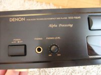
The last pictures show the prepared DENON cd player for testing the PCM1702.
The question whether the difference in the values of the voltage between + Vcc / +Vdd and -Vcc / -Vdd should only remain very small during the start-up phase and during discharge process after switched off is still unanswered.
I guess, this doesn't matter (otherwise the DAC-IC in cd player devices would always fail if one of the positive and negative voltages wasn't present due to a fault in the associated power supply), however, I don't know exactly.
One thing I have discover: there are diodes anti parallel between each supply rail and GND.
BTW - the burned resistors are not interrupted but too small for the power loss (please note, the current flow in the neg. half is much more than in pos. half.) The basic operation and the fact, that the second voltage regulator doesn't matter after start-up phase I had already mentioned in post # 46.
Attachments


Last edited:
UnderThe question whether the difference in the values of the voltage between + Vcc / +Vdd and -Vcc / -Vdd should only remain very small during the start-up phase and during discharge process after switched off is still unanswered.
Question arround the Power Supply of Linn's Preamp LK-1
is the circuit diagram of Linn's preamp LK-1 (post #7).
The open emitters of the accumulation of NPN / PNP transistors controls the on/off mode of ±-voltage from each amp unit (MM-input/MC-input/RIAA-stage/line-stage) independent of each other.
https://www.diyaudio.com/forums/att...-linn-lk1-power-supply-schema-own-drawing-pdf
this could be a good starting point for an additional circuit that only switches the PCM1702 to both supply voltage rails when exactly 5V is present on both the positive and the negative rail.
When switching off, this would also ensure that the 5V is immediately to zero volts again, without the entire range of 5-0V being gradually passed through when the capacitors (2x270.000uF on both halves) are discharged.
Furthermore, a resistor must be introduced between both positive PINs of PCM1702 and GND in order to have the same current consumption as at the neg. half, so that the small capacitances directly at the supply pins of PCM1702 (47-220uF) are discharged at the same speed after switching off.
Last edited:
In several commercial cd players Mitsubishi's M5290P is in use:
M5290P pdf, M5290P description, M5290P datasheets, M5290P view ::: ALLDATASHEET :::
M5290P pdf, M5290P description, M5290P datasheets, M5290P view ::: ALLDATASHEET :::
Due the relatively low cost of the DENON cd player equipped with PCM1702
I risked switch-on the DAC device with the desoldered PCM1702 from those used Denon.
But the left channel still don't work.
After I put it back into the Denon CD player, where I had already inserted a 16-pol socket, I note, this PCM1702 still works perfectly.
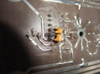
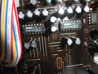
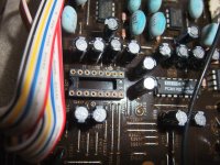
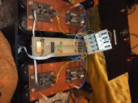
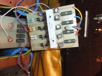
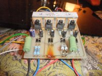
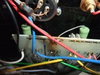
After some measurements it turned out, that on the Horch DAC-PCB is no conductive path from solder side of the board to the component side. I. e. no plated through holes are present. Consequence was the need to introduce additional wire bridges due the additional introduced socket for the PCM1702, which couldn't be soldered from the component side (go to the attached images).
After doing this and replace the burned 270R resistors by 5W versions the Horch DAC device work perfect since several days.
However, I note, that the time is very long after switch-on (approximately 30-35 minutes) until the+/-5V has reached its final value.
The next step is the design of a shunt regulation and a monitoring circuit that connects the supply voltage to the IC when the correct value is available at the big capacitor cans and not before.
In retrospective, the reason for the defect on the old PCM1702 could also have been that the quality of one of the soldered joints at the PCM1702 on component side was poor (which I can no longer determine now).
I risked switch-on the DAC device with the desoldered PCM1702 from those used Denon.
But the left channel still don't work.
After I put it back into the Denon CD player, where I had already inserted a 16-pol socket, I note, this PCM1702 still works perfectly.
After some measurements it turned out, that on the Horch DAC-PCB is no conductive path from solder side of the board to the component side. I. e. no plated through holes are present. Consequence was the need to introduce additional wire bridges due the additional introduced socket for the PCM1702, which couldn't be soldered from the component side (go to the attached images).
After doing this and replace the burned 270R resistors by 5W versions the Horch DAC device work perfect since several days.
However, I note, that the time is very long after switch-on (approximately 30-35 minutes) until the+/-5V has reached its final value.
The next step is the design of a shunt regulation and a monitoring circuit that connects the supply voltage to the IC when the correct value is available at the big capacitor cans and not before.
In retrospective, the reason for the defect on the old PCM1702 could also have been that the quality of one of the soldered joints at the PCM1702 on component side was poor (which I can no longer determine now).
Attachments

Last edited:
The unusual regs may have something going for them, you know. Maybe the designer was hearing something and not just measuring. If you have the schematic for the regs I wouldn't mind looking at it
Your description of the regs reminded me of the regulator shown below, which I have tried with very good results. It improved the sound indeed, and for me it wasn't just an improvement of transients as this fellow wrote:

But what exactly is happening I don't know. To be considered: Increase the load on a regulator and the output impedance goes down, and some other parameters might improve as well.
Also, there is a possibility of a better transfer function of the power transformer with increased load (think of it as a filter and the bandwidth goes down with loading).
These things might play a role, other than the "current direction" explanation that the fellow wrote.
In a semi-parallel regulator, i3 is adjusted to never become negative. Thus, the analog stage is never directly powered by the regulator, this improves transient response. The LT3080 ensures line regulation.
But what exactly is happening I don't know. To be considered: Increase the load on a regulator and the output impedance goes down, and some other parameters might improve as well.
Also, there is a possibility of a better transfer function of the power transformer with increased load (think of it as a filter and the bandwidth goes down with loading).
These things might play a role, other than the "current direction" explanation that the fellow wrote.
Attachments

- Home
- Source & Line
- Digital Line Level
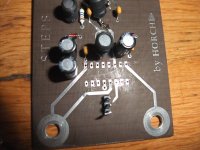
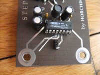
- One of German's most ultimate DAC: Horch "STEPS 1" - Schematic wanted