sorry to be negative, but with this datasheet kind of setup of a DAC with a power amplifier PSU as only "high end thingie" I do not believe this comes close to be of the "most ultimate" dacs....
This is all old school and very much outdated if you really want a great analog sound out of your DAC
If you are not that far from Wiesbaden, feel free to bring it along for a check (after Corona is over...)
This is all old school and very much outdated if you really want a great analog sound out of your DAC
If you are not that far from Wiesbaden, feel free to bring it along for a check (after Corona is over...)
good adviceBUF04 ?
https://www.analog.com/media/en/technical-documentation/obsolete-data-sheets/820549BUF04.pdf
https://www.analog.com/media/en/technical-documentation/obsolete-data-sheets/548191594BUF03.pdf
But one question remains:
What happens, when I connect one of the offset pins (pin1) with Vee (neg voltage pin 4) ?
Maybe this BUF version is the appropriate part, because here pin1 has an other function:
https://www.ti.com/lit/ds/symlink/buf634.pdf?ts=1603196392989&ref_url=https%3A%2F%2Fwww.google.de%2F
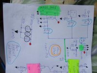
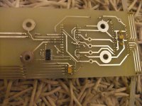
Horch D/A Converter Model STEP - Input Board Schematic
In the attachment several images and own create schematics. Please note - all IC types are just assumptions. Any other pin-compatible versions from those days could just as easily be used.
In the attachment several images and own create schematics. Please note - all IC types are just assumptions. Any other pin-compatible versions from those days could just as easily be used.
Attachments
-
 Input Board-schem.-II.jpg667 KB · Views: 354
 -
 Input Board-schematic.jpg645.2 KB · Views: 349
 -
 Input Board +5Vdig caps.jpg1,000.4 KB · Views: 341
 -
 Input Board-I.jpg1,004.3 KB · Views: 320
 -
 Input Board-III.jpg999.8 KB · Views: 334
 -
 Input Board-V.jpg963.7 KB · Views: 172
 -
 Input Board-VI.jpg952.3 KB · Views: 176
 -
 Input Board +5Vdig-inputs.jpg981.7 KB · Views: 154
 -
 Input Board +5Vdig-inputs-II.jpg979.8 KB · Views: 143
Last edited:
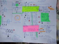
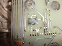
Horch D/A Converter Model STEP - DAC+I/U Board Schematic
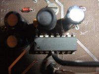
How many pin compatible versions exist from DAC-IC "PCM1702P" and operational amplifier AD844 (60 MHz, 2000 V/μs or better) ?
How many pin compatible versions exist from DAC-IC "PCM1702P" and operational amplifier AD844 (60 MHz, 2000 V/μs or better) ?
Attachments
Last edited:
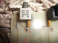
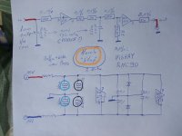
Horch D/A Converter Model STEP - BUF/Low Pass Board Schematic
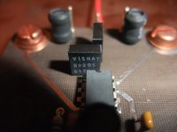
How many pin compatible versions exist from BUF634 (pin1 for confiruartion of the bandwidth and not for offset adjust) ?
How many pin compatible versions exist from BUF634 (pin1 for confiruartion of the bandwidth and not for offset adjust) ?
Attachments
How many pin compatible versions exist from DAC-IC "PCM1702P" and operational amplifier AD844 (60 MHz, 2000 V/μs or better) ?
IF it is AD844 then You can check pin 5 with scope?
Did You fix the issue with one channel?
Why PIN5 ?IF it is AD844 then You can check pin 5 with scope?
Did You fix the issue with one channel?
Yesterday I have find out the the part causing the fault. It is the PCM1702 (PIN11 death).
I have order a cheap DENON DCD755 in used condition. Here I get out a PCM1702 for temporarily test. If the DAC work I will replace again by a high grade version with better performance.
Last edited:
Because pin 5 in AD855 is different from most of other single OPamps. Please refer to AD844 internal structure in pdf?
.
And I am pretty sure that with replacement of DF with PMD100 You will have significant better result?
It is DIP body also but new is maybe hard to find...
.
So it is one of the dac chip fault? Great that You will bring back in operation this device")
.
Did You measure DC offset after the IV OP and after each OPA buffer?
.
One more thing - try to separate digital bus lines between DF board and dac boards? I think that they are longer and have some additional capacitance and crosstalk from that flat multi cable? Just an idea...
.
And I am pretty sure that with replacement of DF with PMD100 You will have significant better result?
It is DIP body also but new is maybe hard to find...
.
So it is one of the dac chip fault? Great that You will bring back in operation this device
.
Did You measure DC offset after the IV OP and after each OPA buffer?
.
One more thing - try to separate digital bus lines between DF board and dac boards? I think that they are longer and have some additional capacitance and crosstalk from that flat multi cable? Just an idea...
Last edited:
Because pin 5 in AD855 is different from most of other single OPamps. Please refer to AD844 internal structure in pdf?
.
And I am pretty sure that with replacement of DF with PMD100 You will have significant better result?
It is DIP body also but new is maybe hard to find...
.
So it is one of the dac chip fault? Great that You will bring back in operation this device
.
Did You measure DC offset after the IV OP and after each OPA buffer?
.
One more thing - try to separate digital bus lines between DF board and dac boards? I think that they are longer and have some additional capacitance and crosstalk from that flat multi cable? Just an idea...
PIN5 of AD844 is the node of VAS-output resp. buffer input. There was no signal in the defective channel. If PMD100 provide better results - I don't know. DC-offset I haven't check. Maybe separate digital bus coax cable (RG179 e. g.) provide better result through reduced jitter level, but this I don't know exactly.
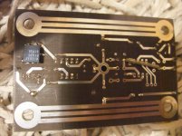
In the attachment additional images.
An interview with the German developer is here:
Interview mit einem Audioentwickler (vorsicht lang!!!, 24 kB)
or
Google Groups
Attachments
-
 2xBUF634+low pass-VI.jpg994.4 KB · Views: 318
 -
 2xBUF634+low pass-VII.jpg979.5 KB · Views: 313
 -
 PCM1702+IU-IV.jpg995.9 KB · Views: 303
 -
 PCM1702+IU-V.jpg985.6 KB · Views: 292
 -
 Input Board-II.jpg964.6 KB · Views: 282
 -
 Input Board-IV.jpg976.6 KB · Views: 109
 -
 Input Board-VII.jpg963.3 KB · Views: 103
 -
 Input Board-VIII.jpg981.8 KB · Views: 106
Last edited:
PCM1702 was fault. I have desoldering this PCM1702 and those from an old DENON cd player. At both places now are sockets for an easy replacement.
After exchanging these ICs the issue was to observe on the DENON - that's the evidence, these PCM1702 is clearly defective.
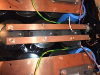
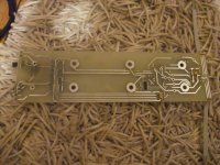
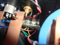
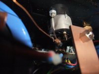
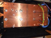
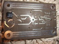
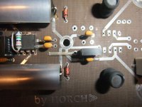
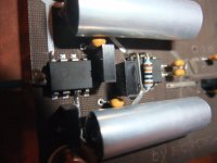
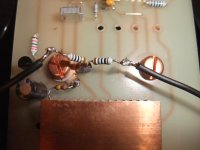
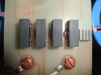
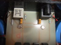
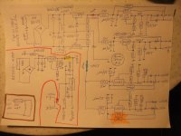
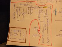
But I can't check the DAC because I observe gross deficiencies on the voltage regulator PCB - go to the attached pictures. After creating the circuit diagram one can see, whats happened exactly for the reason of burned resistors.
After exchanging these ICs the issue was to observe on the DENON - that's the evidence, these PCM1702 is clearly defective.
But I can't check the DAC because I observe gross deficiencies on the voltage regulator PCB - go to the attached pictures. After creating the circuit diagram one can see, whats happened exactly for the reason of burned resistors.
Attachments
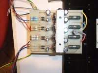
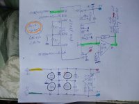
I have never seen before this approach of voltage regulation - it confuses me. Basically, there are two series regulators connected in series. The second series regulator generating a stabilized voltage that is below the desired values - go to the attached circuit diagram.
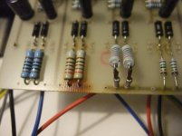
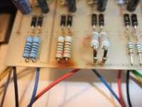
The desired values are obtained by connecting resistors of a certain value in parallel to the second voltage regulator, which are adjusted to the individual power consumption both of the DAC and high pass filter/buffer modules.
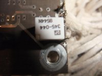
The marked 270R resistors are overheated but not defective.
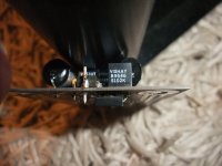
The series diodes prevent voltage from flowing back into the output of the second regulator, unfortunately not in the first regulator because of the resistors connected in parallel to the second regulators (please note - behind the output of the second regulator stages are connected very large capacities of approximately 400.000µF/each rail - outside of the capacitors are nothing to read).
I want to create a parallel regulator resp. shunt regulator concept.
What needs to be considered here ?
Thanks for an advice and calling the appropriate topics here on diyaudio.
The desired values are obtained by connecting resistors of a certain value in parallel to the second voltage regulator, which are adjusted to the individual power consumption both of the DAC and high pass filter/buffer modules.
The marked 270R resistors are overheated but not defective.
The series diodes prevent voltage from flowing back into the output of the second regulator, unfortunately not in the first regulator because of the resistors connected in parallel to the second regulators (please note - behind the output of the second regulator stages are connected very large capacities of approximately 400.000µF/each rail - outside of the capacitors are nothing to read).
I want to create a parallel regulator resp. shunt regulator concept.
What needs to be considered here ?
Thanks for an advice and calling the appropriate topics here on diyaudio.
Attachments
Last edited:
What reviews ? I don't know about reviews in any German magazine.Maybe, I've missed something, but the schematics don't appear to show why this would be considered Germany's ultimate DAC. Rather, seeming quite average.
I can't read the German reviews, so, perhaps you can clarify?
- Home
- Source & Line
- Digital Line Level
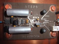
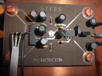
- One of German's most ultimate DAC: Horch "STEPS 1" - Schematic wanted