If they thought it would sell at lower frequencies then why not show it in the data sheet? That doesn't seem odd for an opamp? If it were a transistor then sure, that could be.
One thing that is not unusual for devices optimized for HF is they may have a high 1/f noise corner. Don't know about this particular device, but my gut feeling is it doesn't smell right.
Noise is shown at low frequencies, though.
I guess I'm confused? I'm still very puzzled by your gut feeling that something is fishy. I did a sampling of the ADA-coded high speed opamp datasheets and the 4806 and 4350 distortion plot starts at 1k, a couple others start at 100k. Don't see what's fishy, probably more what they had set up on the bench when they ran the test suite. All show lower distortion at lower frequencies, as we'd expect.
But, hey, I can hardly wait for one of you guys to build a ES9038Q2M DAC with it and do A/B comparisons with the opamps ESS recommends. However, I don't think we should be giving newbies the idea that they should be the ones to try it first if they want a good DAC and are putting a lot of work and some money into it. That's all. If one or two of the knowledgeable and experienced people want to do it to show the beginners how one should do such testing that would be great. Good learning opportunity for them to watch your progress as you build and test it. Please post plenty of pics if you would be so kind, I am sure the beginners would appreciate all they can learn from you.
Snarkiness aside (I started it, to be fair), I agree that I wouldn't want inexperienced folks to run off and use the ADA4898 right away. At the same time, I don't think it's somehow suspicious because it doesn't have an low frequency AP distortion plot.
I'll let my buddy know who's in AD's scientific instruments(ish) department as technical sales and marketing that I'd love my cut. ")
(He was at National before TI bought them)
You'll please note that I recommend the 497x0 as much as possible. People respect your opinion, and making jumps off suspicion in a sea of contradictory evidence and basic device fundamentals isn't doing anyone any good.
(He was at National before TI bought them)
You'll please note that I recommend the 497x0 as much as possible. People respect your opinion, and making jumps off suspicion in a sea of contradictory evidence and basic device fundamentals isn't doing anyone any good.
People respect your opinion, and making jumps off suspicion in a sea of contradictory evidence and basic device fundamentals isn't doing anyone any good.
If that is true, then I probably should have been a little more careful with my words in this case. However, I'm not sure I knew at the outset why my System 1 was giving me warning intuition. After thinking about it a little more I think it was mostly that concern about newbies, given what is involved in doing all the mods well. As an intellectual exercise, I don't see a problem with the logic applied to what the performance is likely to be at below 100kHz. But, I can't see anyone investing in a lot of effort to mod a DAC experimentally when a workable solution with very good results has already been found. If somebody wants to work on an interesting problem, how about SOA I/V conversion for ES9038PRO given the higher output currents?
Hey, agree that the 4898 (and the 497x0 for that matter) is an opamp that can get sideways on you really quick and become a fine variable and uncontrolled oscillator, whereas we have a really good solution already here, saving a couple bucks in the process. Both are high performers, albeit with the noted RF sensitivity on a 497x0 attached to an antenna (or not in box).
Pretty sure I'd want a discrete input, probably a hybrid opamp + common-base/gate to handle the kind of current the 9038PRO can swing. That's a lot of juice to push. Fun problem, but not one I'm pursuing. Fun thought exercise nonetheless.
Pretty sure I'd want a discrete input, probably a hybrid opamp + common-base/gate to handle the kind of current the 9038PRO can swing. That's a lot of juice to push. Fun problem, but not one I'm pursuing. Fun thought exercise nonetheless.
I have a Chinese SRC4392. Its plenty good enough, I think. Appears to be a genuine SRC4392 chip, and sounds like it too.
To take control of the chip via I2C at some point though will involve tapping into a couple of tiny traces or IC pins on the board. It is quite doable, again I think, although I haven't done this one yet. There are various ways of going about it. I could post some tips and instructions if that's what people need to feel comfortable they can do it.
The only other issue might be the clock quality. I don't know if it will be an issue or not until I get the DAC chip datasheet and start working on master mode I2S. However, the clock could be an issue no matter which one you buy, even a development board from TI. Nobody puts ultra-low jitter clocks on general purpose boards. Such clocks are only for very high-performance systems.
If you did buy a TI development board which I have looked into, they are easy to interface to, bring out all the chip I/O functionality, don't have exceptionally good clocks, are not small, and do not ease learning how to program the chip at all. Cost for that is about $150 vs $60 for the Chinese board. Clock jitter might potentially even be better on the Chinese board than the TI development board, since on the Chinese board the clock is physically located very close to the SRC chip.
As far as using an SRC4392 or not, they make a key difference. It is essential to getting close to DAC-3 or Crane Song 5th generation DAC sound quality. All IMHO, of course. But trust me, it helps a lot even without master mode I2S. You would want to have it if you heard it.
Mark is correct here. When the DAC is close to optimal, the SRC is easily discernable when used.

Well, I'm a beginner and I simply don't have experience of listening to both valve and SS systems, so I'm not in a position to make any firm statements, in fact, I'm conscious of how little I know and therefore am happy to be guided and follow advice - that's why I joined the forum!
Can anyone point me to a SS solution for an analogue output stage, preferably a nice, simple one, so I can do some studying and try to gain a better understanding.
Is it possible to buy a suitable output stage as a ready made item, or is it a case of having to buy the op amp chips and other parts and build your own?
I'm tempted to build both a SS and a valve solution so I can try both and see which sounds better to my eyes, as I get the impression there is a lot of subjectivity and personal taste involved.
You might want to go back and look at the pictures here: http://www.diyaudio.com/forums/digital-line-level/314935-es9038q2m-board-84.html#post5415832
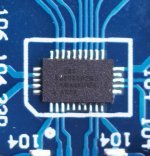
There is also a picture of the pinout diagram for the DAC chip here:
ES9038Q2M Board
The thing about the pictures is that they are high resolution but when you click on them you don't see full detail. So, to look at one click on it to open it, then while it is open hover the mouse over the lower left corner where a white X should appear. Clicking on the white X should expand the pictures up to full size. Or, you can right click on the pictures when they are open to select to download them. Then you can look at them in whatever picture viewing app you like to use.
Anyway, one picture shows the dac board with labels on some of the parts. It needs to be viewed at full size to read all the labels. That should help understand what all the parts on the board are for.
The way I modified the DAC board was to mount some mods on the bottom side of the DAC board. There is a special ultra-clean power supply for something called AVCC, a voltage that is super critical for good dac operation. Also on the bottom are the IV or current to voltage converters. The bottom also has a couple of 3.3v voltage regulators, one as a reference for AVCC, and one to power the clock. I might have done that part a little differently. Maybe the pins on the DAC chip labeled VCCA could have been powered by the same regulator as the clock.
On the top of the board the area where the socket is has been modified to make it into a differential amplifier to sum the IV outputs into Left and Right stereo outputs.
Also on the top of the board the clock oscillator module has been replaced.
In addition the 5v regulator was replaced, although currently I am not using that for 5v power, I am using an external 5v supply instead.
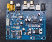
The latest test setup includes external power supplies, a headphone amp which I recommend building, and a couple of sample rate converters to compare. A picture is here: http://www.diyaudio.com/forums/digital-line-level/314935-es9038q2m-board-165.html#post5477499
The thing I would suggest doing would be to familiarize yourself with the board and the parts on it, and also read and study some documents ESS provides that help explain how to make a good dac. Those files can be found here: ESS Technology :: Downloads The most important document which should be studied carefully and even notes taken is the one entitled, " Maximizing DAC Performance for Every Budget."
Okay. Once you have a look at everything then we can start talking about details. During that process you might want to download and read some datasheets for parts you would be working with.
As you can see even though it is one simple looking little board, to make it into something pretty near to state of the art, but not quite there, is a fair undertaking. Lots to look at and think about to decide how you would like to proceed. For one thing, to do some of the work you may find you could make good use of a few tools you may or may not already have. A solder iron with a very small tip and a temperature control knob is pretty important. A good head-mounted magnifier or even a lower-cost soldering microscope can be helpful depending on how your vision is. Small wire cutters, tweezers, non-locking ophthalmic needle holder, etc., can be very helpful.
There is also a picture of the pinout diagram for the DAC chip here:
ES9038Q2M Board
The thing about the pictures is that they are high resolution but when you click on them you don't see full detail. So, to look at one click on it to open it, then while it is open hover the mouse over the lower left corner where a white X should appear. Clicking on the white X should expand the pictures up to full size. Or, you can right click on the pictures when they are open to select to download them. Then you can look at them in whatever picture viewing app you like to use.
Anyway, one picture shows the dac board with labels on some of the parts. It needs to be viewed at full size to read all the labels. That should help understand what all the parts on the board are for.
The way I modified the DAC board was to mount some mods on the bottom side of the DAC board. There is a special ultra-clean power supply for something called AVCC, a voltage that is super critical for good dac operation. Also on the bottom are the IV or current to voltage converters. The bottom also has a couple of 3.3v voltage regulators, one as a reference for AVCC, and one to power the clock. I might have done that part a little differently. Maybe the pins on the DAC chip labeled VCCA could have been powered by the same regulator as the clock.
On the top of the board the area where the socket is has been modified to make it into a differential amplifier to sum the IV outputs into Left and Right stereo outputs.
Also on the top of the board the clock oscillator module has been replaced.
In addition the 5v regulator was replaced, although currently I am not using that for 5v power, I am using an external 5v supply instead.
The latest test setup includes external power supplies, a headphone amp which I recommend building, and a couple of sample rate converters to compare. A picture is here: http://www.diyaudio.com/forums/digital-line-level/314935-es9038q2m-board-165.html#post5477499
The thing I would suggest doing would be to familiarize yourself with the board and the parts on it, and also read and study some documents ESS provides that help explain how to make a good dac. Those files can be found here: ESS Technology :: Downloads The most important document which should be studied carefully and even notes taken is the one entitled, " Maximizing DAC Performance for Every Budget."
Okay. Once you have a look at everything then we can start talking about details. During that process you might want to download and read some datasheets for parts you would be working with.
As you can see even though it is one simple looking little board, to make it into something pretty near to state of the art, but not quite there, is a fair undertaking. Lots to look at and think about to decide how you would like to proceed. For one thing, to do some of the work you may find you could make good use of a few tools you may or may not already have. A solder iron with a very small tip and a temperature control knob is pretty important. A good head-mounted magnifier or even a lower-cost soldering microscope can be helpful depending on how your vision is. Small wire cutters, tweezers, non-locking ophthalmic needle holder, etc., can be very helpful.
Yes. If you don't like building and modding, this might not be the right way for you to go.
However, if lampizator is simple then why is it expensive? It probably requires of lot of support circuitry to work well, things like exceptionally good power supplies that cost way more to make than the simple triode part.
EDIT: There is also a digital dac board that probably has the usual concerns in terms of power, reference voltages, low-jitter clocking, and so forth. The basic valve output may be simple looking on paper, but they use a particular type of valve and power supply or supplies for it. Starting with a cheap dac board still might require some work on that board to get it ready to perform well with the valve stage.
Last edited:
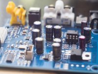
My DAC board just arrived in the mail, I have to say, it has a very cheap feel to it. There's only one op amp and it's socketed.
I'm suspicious that this is a fake knock-off rather than an actual ES9038 chip as it's unmarked and looks nothing like the pictures of the ES9038 IC I've seen.
I'll post pics shortly.
I'm suspicious that this is a fake knock-off rather than an actual ES9038 chip as it's unmarked and looks nothing like the pictures of the ES9038 IC I've seen.
I'll post pics shortly.
Looking at the DIY lampizator website there is this download that shows interfacing to a current output DAC chip http://lampizator.eu/LAMPIZATOR/photogallery/STEPS/Lampizator.doc
Basically, they do it kind of like the transformer output guys do, with current sensing shunt resistors. Even if using tubes, for this scheme to work with Sabre dacs probably better to use transformers followed by tubes since these dacs have differential outputs that need to be subtracted. Also there is the matter of the reference voltage offset which is ignored by the transformer guys. If using valves, it would still take one dual triode per dac channel phase or 4 sets of stacked triodes then followed by two differential subtraction circuits. Basically, valve op amp circuits. Probably easier to do with voltage output dac chips not ESS Sabre type chips. However, at least the ES9038PRO puts out enough current the current sense shunt resistors might generate more of a voltage signal for the valves to amplify.
Anyway, in short I would say doing a good lampizator type circuit and doing it well with Sabre dacs would be just as complicated as using opamps, probably more so actually. On the other hand, doing a poor quality version with poor sound quality might be simple.
Of course, the ultimate simplicity is to buy a pre-built DAC to suit your tastes. Maybe the complexity would be in digging up the cost of a really good one.
Last thing is I think in terms making a really good DAC for you, I don't know about others, but I could only really offer much in the way of help if you wanted to work on something like what was in the pictures I linked to. That's what I have done with a Sabre DAC all the way through that I know works. There are no remaining problems that we haven't figured out how to take care of. By listening and or measuring it does what it is supposed to and the sound quality is exceptionally good. But, as you can see, it is a lot of work. Maybe Mikett over in his thread can offer you an easier path, although I don't know if he has settled on an endpoint for his project as much as we have here. That thread is in this sub-forum area here: Moving from 9038Q2M to a 9028Pro board
I'm suspicious that this is a fake knock-off rather than an actual ES9038 chip as it's unmarked and looks nothing like the pictures of the ES9038 IC I've seen.
It should be a Q2M chip like you saw in the pictures I linked to. They are small and rectangular, not bigger and square like the PRO chips. To read the laser marking on chips sometimes it takes a magnifying glass and a flashlight held at an angle to see it. That isn't uncommon.
Well, I was wrong, it is marked, just very hard to see with the naked eye, I could only see it when I looked at the digital photo I'd taken of the board.
Here's the pics:
Here's the pics:
Attachments
Looking at the DIY lampizator website there is this download that shows interfacing to a current output DAC chip http://lampizator.eu/LAMPIZATOR/photogallery/STEPS/Lampizator.doc
Basically, they do it kind of like the transformer output guys do, with current sensing shunt resistors. Even if using tubes, for this scheme to work with Sabre dacs probably better to use transformers followed by tubes since these dacs have differential outputs that need to be subtracted. Also there is the matter of the reference voltage offset which is ignored by the transformer guys. If using valves, it would still take one dual triode per dac channel phase or 4 sets of stacked triodes then followed by two differential subtraction circuits. Basically, valve op amp circuits. Probably easier to do with voltage output dac chips not ESS Sabre type chips. However, at least the ES9038PRO puts out enough current the current sense shunt resistors might generate more of a voltage signal for the valves to amplify.
Anyway, in short I would say doing a good lampizator type circuit and doing it well with Sabre dacs would be just as complicated as using opamps, probably more so actually. On the other hand, doing a poor quality version with poor sound quality might be simple.
Of course, the ultimate simplicity is to buy a pre-built DAC to suit your tastes. Maybe the complexity would be in digging up the cost of a really good one.
Last thing is I think in terms making a really good DAC for you, I don't know about others, but I could only really offer much in the way of help if you wanted to work on something like what was in the pictures I linked to. That's what I have done with a Sabre DAC all the way through that I know works. There are no remaining problems that we haven't figured out how to take care of. By listening and or measuring it does what it is supposed to and the sound quality is exceptionally good. But, as you can see, it is a lot of work. Maybe Mikett over in his thread can offer you an easier path, although I don't know if he has settled on an endpoint for his project as much as we have here. That thread is in this sub-forum area here: Moving from 9038Q2M to a 9028Pro board
I very much appreciate your being so patient with me, being a total beginner, I expect I am asking some questions that seem quite silly.
There is a page about adding a Lampizator to the older versions of the Sabre DAC, he says it was very easy with the Buffalo board he used:
BuffaloDAC
I'm not at all tied to the idea of copy the lampizator or even using valves, I just found it simple to understand with my limited knowledge.
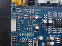
Regarding the board you just received, it looks like they are trying to get people to run it from a single ended +12v supply. I marked up the picture you took to show where positive, negative, and ground would be connected to a dual rail +-12v or +-15v power supply. I also put a red X where a trace would need to be cut, as it connects the negative rail to ground which would be needed if using a single +12v supply. The other green board similar to the blue one you have comes the with the power configured the other way around as the default, with a jumper that needs to be soldered in if using a single supply.
Attachments

Last edited:
Regarding the board you just received, it looks like they are trying to get people to run it from a single ended +12v supply. I marked up the picture you took to show where positive, negative, and ground would be connected to a dual rail +-12v or +-15v power supply. I also put a red X where a trace would need to be cut, as it connects the negative rail to ground which would be needed if using a single +12v supply. The other green board similar to the blue one you have comes the with the power configured the other way around as the default, with a jumper that needs to be soldered in if using a single supply.
yes, even "made in china" gets knock-offs .... the original ones have version numbers though.
Regarding the board you just received, it looks like they are trying to get people to run it from a single ended +12v supply. I marked up the picture you took to show where positive, negative, and ground would be connected to a dual rail +-12v or +-15v power supply. I also put a red X where a trace would need to be cut, as it connects the negative rail to ground which would be needed if using a single +12v supply. The other green board similar to the blue one you have comes the with the power configured the other way around as the default, with a jumper that needs to be soldered in if using a single supply.
Hi i have exactly the same board. I will check in the evening what I modified to Be able to handle the symmetric ps. As I remember I had to modify the OPA stage a littlebit the 12v was devided to half for a virtual ground.
It can be connected to the real ground.
- Home
- Source & Line
- Digital Line Level
- ES9038Q2M Board