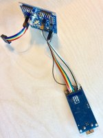
Received my AK4137 the newer one. Since my DAC has USB I2S headers for USB XMOS, I imagine the AK4137 board simply interposes between the XMOS and the DAC USB headers.
Looks to be a male, female arrangement.
What is the best way to do this? Would a 20 pin double row ribbon do the trick?
Just came across the idea of using an ATA 100 IDE cable. https://allpinouts.org/pinouts/cables/data_storage/ultra-ata-66-100-ide/
Using the half that does not have the detection connection. I have some of these older cables and to create the male end I would simply insert a male to male coupler in between. Any thoughts anyone?
Last edited:
Received my AK4137 the newer one. Since my DAC has USB I2S headers for USB XMOS, I imagine the AK4137 board simply interposes between the XMOS and the DAC USB headers.
Looks to be a male, female arrangement.
What is the best way to do this? Would a 20 pin double row ribbon do the trick?
Just came across the idea of using an ATA 100 IDE cable. https://allpinouts.org/pinouts/cables/data_storage/ultra-ata-66-100-ide/
Using the half that does not have the detection connection. I have some of these older cables and to create the male end I would simply insert a male to male coupler in between. Any thoughts anyone?
Mike,
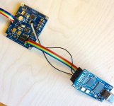
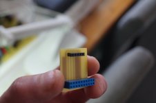
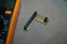
The trouble with using a pre-built ribbon cable is that they are too long for what we need and they don't typically use gold contact points inside. We want the cable from AK4137 output to be 3" long or less. The very shortest possible, and we want gold pins and gold female connectors on the ribbon. The main reason for having any connector at all is for convenience so we can take things apart later if we want.
What I did in one case was solder one end of a short ribbon to the bottom side of the pin connector at AK4137 board output, then install a gold two row pin connector for the dac I2S input. That required drilling some extra holes for the ground row so those pins could solder to the dac board ground plane.
I have also removed existing pins from AK4137 boards and drilled some extra holes for ground pins. In some cases I couldn't find a way to put all the pins in neat rows with grounds all on one side so I had to figure out something else. Please see pics below for one example. Yellow pins in pics are added ground pins.
Computer buses can be fast, but they don't care about low-ish femtosecond level jitter like we do.
To make up the female end of the ribbon cable I found some gold crimp pins and bought a crimp tool. Each female pin is crimped, then soldered, then carefully checked and reshaped a little if necessary with small pliers so it can be inserted into the female pin housing. It is tedious work, and since the time I bout the crimp connector kit, the kits with gold pins seem to have disappeared from the market (although the male/female gold crimp inserts can be bought one pin at a time from Mouser). Since female gold crimp pins are not cheap, I practiced with standard tin pins until I could make up the connectors reliably. The tin pin kits are something like: https://www.amazon.com/Glarks-Conne...n+header+kit&qid=1568901922&s=gateway&sr=8-10 ...and there used to be a couple of gold plated kits like that on Amazon at one time. The Chinese kits have crimp pins made out of thin-ish metal compared to the much more expensive pin inserts at Mouser, IME. However, the Chinese kits are workable if one with gold pins can be found.
Attachments
Last edited:
Also, i've drawn a technical drawing from MrSlim's schematic.
I apologize if its a bit messy (i admit, space management wasnt the best), but maybe it helps someone with the modding.
(if you have the time or will, can you tell if something is wrong so people dont look at it in case there's a mistake)
P.S, the R50-53 resistors for the balanced output are 0 ohm, i.e deprecated?
Higher res link (imgur)
Zbunjen,
No offense intended my friend, but the drawing you made is not useful for what we do in electronics. It is neither a readable schematic, nor a proper layout diagram.
Schematics should look like the ones MrSlim drew, where signal flow is left to right, higher positive voltages are at the top, negative voltage rails at the bottom, and unnecessary crossing lines are minimized by using ground symbols and other symbols showing connections to power rails, etc. Standard symbols should be used for components such as opamps.
On the other hand, for layout diagrams we need much more information about the physical location of components and the physical path that interconnections take. There is nothing that says wires can't pass under opamps or between the pins of opamps, there is no need for wires to make square corners around opamps in most cases. I sometimes draw up a layout diagram on graph paper with each grid-line intersection representing a hole in a perfboard. In that case the drawings are to scale as mechanical drawings should be. Also, I use a ground plane in most cases so there is no single ground line running through the circuit. Usually, there are not single power rails running around either. I try to route the power sensibly depending on where currents are flowing. Where wires must cross, I used colored pencils to draw the wires so it is easier to read.
Something we need to memorize is that pin numbers on devices are numbered clockwise from pin 1 when looked at from the top. We must get used to knowing that pin numbers are counterclockwise from the bottom starting from pin 1. With though-hole PCBs, it is fairly standard to pin 1 to be indicated with a square solder pad, and with round solder pads used for all the other pins. That makes it easy to keep track of pins from the bottom of a board. With some practice, there is no need to draw opamps as boxes except for on layout diagrams, which are more or less mechanical drawings for all components and wiring.
Last edited:
Hey, none taken Mark.Zbunjen,
No offense intended my friend, but the drawing you made is not useful for what we do in electronics. It is neither a readable schematic, nor a proper layout diagram.
 Was kind of expecting this, since i was winging it for the most part (my background is in software development, this was probably my first schematic in the last 10 years). I appreciate the honesty too.
Of course, paper being a 2D medium there is no way to show what is actually possible layout wise on a perfboard which has benefits of three dimensionality, where i can already visualise that ill run some wires from underneath to keep it tight (and not in square shapes). If i were to draw the lines as they would be as a topographical projection of the physical board onto the paper, it would be about 15x10cm (guesstimate) drawing and all the wires would be running trough trough all the components left and right, i wouldn't make out what is what in such a scenario.On the other hand, for layout diagrams we need much more information about the physical location of components and the physical path that interconnections take. There is nothing that says wires can't pass under opamps or between the pins of opamps, there is no need for wires to make square corners around opamps in most cases. I sometimes draw up a layout diagram on graph paper with each grid-line intersection representing a hole in a perfboard. In that case the drawings are to scale as mechanical drawings should be. Also, I use a ground plane in most cases so there is no single ground line running through the circuit. Usually, there are not single power rails running around either. I try to route the power sensibly depending on where currents are flowing. Where wires must cross, I used colored pencils to draw the wires so it is easier to read.
I saw this principle in your dropbox schematic, yeah. The only reason i twisted them is because on MrSlim's schematic the -15v runs from pin 4 upwards and +15v from pin 8 downwards, so instead of rotating the whole schematic i just rotated the DIP to match the trajectory.Something we need to memorize is that pin numbers on devices are numbered clockwise from pin 1 when looked at from the top. We must get used to knowing that pin numbers are counterclockwise from the bottom starting from pin 1. With though-hole PCBs, it is fairly standard to pin 1 to be indicated with a square solder pad, and with round solder pads used for all the other pins. That makes it easy to keep track of pins from the bottom of a board. With some practice, there is no need to draw opamps as boxes except for on layout diagrams, which are more or less mechanical drawings for all components and wiring.
Received my AK4137 the newer one. Since my DAC has USB I2S headers for USB XMOS, I imagine the AK4137 board simply interposes between the XMOS and the DAC USB headers.
Looks to be a male, female arrangement.
What is the best way to do this? Would a 20 pin double row ribbon do the trick?
Just came across the idea of using an ATA 100 IDE cable. https://allpinouts.org/pinouts/cables/data_storage/ultra-ata-66-100-ide/
Using the half that does not have the detection connection. I have some of these older cables and to create the male end I would simply insert a male to male coupler in between. Any thoughts anyone?
I've used an old IDE cable and even a nicely shielded SATA cable, just keeping the lengths at the minimum/workable lengths.
I've put my AK4137 to one side at present, using the upsampling capability of Roon and then using DSD 2.82 (DoP) over coax from my Allo DigiOne RPi. It will be interesting to compare the results at a point in time when I stop fiddling with this board.
Well, I've started to 'remove' some of the old SMD components, replacing these will pin connectors so I can disassemble and move the boards around easily. I've got the two AVCCs 'fed' with an op-amp regulated 3.3v (LT3045), the next to change is the power to the other ancillaries (DVCC, VCCA, clock etc) in line with what I did before. Question for Mark (and others) is there any benefit in op-amp regulating the other VCs before I just use another LT3045.
Thanks to diyaudio I took advantage of the Salas UltraBiB group buy and I'm now powering the DAC with three of these UBiBs (+/- 15v and 5v...well 7v until I replace the 7805) replacing the LM317 and LT1963.
I'm very pleased with the results of this, just goes to emphasise just how important the power supply really is!
Last edited:
...Question for Mark (and others) is there any benefit in op-amp regulating the other VCs before I just use another LT3045...
No reason to use opamp voltage regulators for anything other than AVCC. Probably best to avoid them for VCCA, DVCC, and clock.
For the output stage using a good quality +-15v shunt regulator should be fine. For shunt regulators with big electrolytic output filter caps, it may turn out that film caps located right at the opamps will help reduce any bit of remaining graininess to the sound. However, for regulators with high loop gain, adding caps to the output may adversity affect stability, possibly causing ringing on transients and or oscillation. If that happens, best to remove added caps and seek further advice.
For VCCA, DVCC, and clock, it is better to use LDO regulators located very close to the loads, ideally located right on the dac board ground plane (to keep all wiring inductance as low as possible for the HF/RF circuitry). LT3045 can be used, or I happened to use LT1763 (with the optional .01uf bypass cap, and with the LDO and associated caps soldered to the back side of the dac ground plane). There are a number of other fairly similar LDO regulators, any of which would probably work fine so long as data sheet recommendations are followed and they are located close to the loads.
Note: It often helps regulator performance to have more than the minimum voltage across the regulator (input to output v), although that may not be explicitly stated on data sheets. It tends to show up in graphs of PSRR verses input to output voltage differential, but it also may have applicability to load regulation.
Last edited:
No reason to use opamp voltage regulators for anything other than AVCC. Probably best to avoid them for VCCA, DVCC, and clock.
For the output stage using a good quality +-15v shunt regulator should be fine. For shunt regulators with big electrolytic output filter caps, it may turn out that film caps located right at the opamps will help reduce any bit of remaining graininess to the sound. However, for regulators with high loop gain, adding caps to the output may adversity affect stability, possibly causing ringing on transients and or oscillation. If that happens, best to remove added caps and seek further advice.
For VCCA, DVCC, and clock, it is better to use LDO regulators located very close to the loads, ideally located right on the dac board ground plane (to keep all wiring inductance as low as possible for the HF/RF circuitry). LT3045 can be used, or I happened to use LT1763 (with the optional .01uf bypass cap, and with the LDO and associated caps soldered to the back side of the dac ground plane). There are a number of other fairly similar LDO regulators, any of which would probably work fine so long as data sheet recommendations are followed and they are located close to the loads.
Note: It often helps regulator performance to have more than the minimum voltage across the regulator (input to output v), although that may not be explicitly stated on data sheets. It tends to show up in graphs of PSRR verses input to output voltage differential, but it also may have applicability to load regulation.
Thanks Mark, above and beyond as usual, an asset to diyAudio!
It's interesting what you are saying about regulator minimum voltage, I'll take that onboard.
I'll have a look at the LT1763, the S8 package seems to lend itself better for the job, having more GND pins to solder onto the ground plane. I'll just make sure to practice with a similarly sized chip on my 'practice' boards!
Damian and Mark, thanks for the suggestions. Since I will be mounting my AK4137 in another case, then I will have to live with a cable and the easiest to get started is with a ribbon. I will attempt the ATA 133 as well and see if there is a difference. That cable has an extra gound line per pin and was supposed to allow better timing and signal integrity over a standard ribbon. I will have to get invetive to get the cable lengths down short though.
I even thought of the SATA cable as well !
I even thought of the SATA cable as well !
Damian and Mark, thanks for the suggestions. Since I will be mounting my AK4137 in another case, then I will have to live with a cable and the easiest to get started is with a ribbon. I will attempt the ATA 133 as well and see if there is a difference. That cable has an extra gound line per pin and was supposed to allow better timing and signal integrity over a standard ribbon.
Anything more than short length wires would tend to be problematic to some degree or other. The LVCMOS circuitry in dac chips, clock modules, and AK4137 can't output enough current to drive a low impedance transmission line. That is the main reason to keep wires very short, not just because of antenna effects. When wires are short enough not to act like transmission lines then what matters is their capacitance, and LVCMOS can't put out enough current to charge up much capacitance either. You may or may not get a usable signal at the far end of the wire, and if you do get a marginally workable signal, the digital waveform fast edges will likely be in pretty bad rounded-off shape. Best chances to work well might be if the two equipment cases could be snug up against each other so AK4137 output is right next to dac board I2S input, with a slot in each case for the cable to pass through. Even better, get a bigger case and put it all in there.
Maybe a good idea to open up the dac case and connect AK4137 right next to the dac for test. See if you even like it.
If you really have to drive transmission lines from one case to the other, you could convert the AK4137 output signals to LVDS, go through the wire, and then convert back to LVCMOS at the dac end, or else maybe use source terminated 50-ohm compatible clock buffer chips for each AK4137 output to drive the lines. LVDS can go much longer distances, but will add significantly non-trivial jitter.
Last edited:
AK4499 Update
Just a few words about AK4499 eval board progress.
Turns out that 'ESS Hump' fix method also seems to help some with AK4499. As usual, and IMHO, the effects probably has more to do with the output stage opamps than the dac chip.
Also, found that despite a couple passive RC filters after the I/V opamp outputs, there still seems to be a little RF leakage coming out of the dac board balanced outputs. If I use a short-length low-capacitance XLR cable from the dac outputs to the Neurochrome HP-1 inputs I start to hear more distortion that sounds rather like RF getting into the opamps. Turns out the differential receiver used for HP-1 balanced inputs is OPA1612, the exact same opamp we would probably use for differential summing inside a completed dac design. A longer piece of the same type of cable seems to exhibit more of an RF filtering effect whereby distortion at HP-1 output is less. While the evidence for low-level RF in the dac outputs is very circumstantial now, the observations described above make me think I have some more work to do to further attenuate RF after the I/V stage.
Another update item is that some additional shielding between the USB board and the dac chip daugherboard area also seems to help reduce some distortion and reduce some blurring of low level ambiance sounds.
Right now the dac is on multiple power supplies and regulators. As usual IME with dac chips so far, using dedicated voltage regulators for different subsystems as much as possible helps sound quality very noticeably. AKM provided banana jacks and jumpers on the eval board to make testing with separate power supplies easier. One thing they missed was making the I/V opamp power separable from the overall dac board +-15v rails. That's probably because they were worried about the risk of destroying the dac chip if power is sequenced incorrectly. There is a warning about that in the AK4499 data sheet. The concern is mainly from the I/V opamp outputs going higher than +7v or so while the dac chip is otherwise powered off. As a result I have had to make sure my power supply design is fail-safe enough to keep the dac chip safe. Bottom line is that it has been worth the trouble in order to keep finding improvements to sound quality though multiple power supplies/regulators.
Are separate transformers really necessary as well as separate preregs and regs??
Don't know. Still experimenting.
Do you know any similar turn on characteristics that could endanger the ESS DAC chips as well?
Only thing I know about is the issue with '5v tolerant' pins which we have talked about before.
Im currently making the AVCC, using the LT3042 as the power supply.
The problem is, i might be the only person the internet to not be able to get these to work.
For 3.3V output i put a 33.2kOhm resistor and a 4.7uF capacitor in parallel to ground from the SET pin.
I get 12V on the input, 0 on the output. I think ok, maybe the Vin-Vout is a bit much, i try it with a 5V supply, nada. The output is like 0.02V.
Hell, i even tried plugging it in backwards thinking something might be labeled wrong ( i was confident given that it has input reverse polarity protection), just no life out of them. I have 2 of these units and neither seem to work. I checked the DC input and its present.
I checked it with an infrared thermometer and it does go 2-3C above room temperature, indicating the magic pixies are getting in there.
The only thing i can think of is i used electrolitic decoupling caps where the spec sheet calls for ceramic (i couldnt get 4.7uf ceramics).
Any ideas? I might be just missing something simple, maybe some other pin needs to be tied to ground..
The problem is, i might be the only person the internet to not be able to get these to work.
For 3.3V output i put a 33.2kOhm resistor and a 4.7uF capacitor in parallel to ground from the SET pin.
I get 12V on the input, 0 on the output. I think ok, maybe the Vin-Vout is a bit much, i try it with a 5V supply, nada. The output is like 0.02V.
Hell, i even tried plugging it in backwards thinking something might be labeled wrong ( i was confident given that it has input reverse polarity protection), just no life out of them. I have 2 of these units and neither seem to work. I checked the DC input and its present.
I checked it with an infrared thermometer and it does go 2-3C above room temperature, indicating the magic pixies are getting in there.
The only thing i can think of is i used electrolitic decoupling caps where the spec sheet calls for ceramic (i couldnt get 4.7uf ceramics).
Any ideas?
I might be just missing something simple, maybe some other pin needs to be tied to ground..
Last edited:
..... and what about EN pin?
and those ebay boards already have a set resistor and a cap. I think the only thing you need is to solder a jumper between VIN and EN. with 12V in the regs will be very hot.
actually I would advice first to study the layout of any board you are touching before trying to reverse the polarity or doing something similar...
Last edited:
..... and what about EN pin?
and those ebay boards already have a set resistor and a cap. I think the only thing you need is to solder a jumper between VIN and EN. with 12V in the regs will be very hot.
actually I would advice first to study the layout of any board you are touching before trying to reverse the polarity or doing something similar...
You're right on all points.
I cant believe my reading comprehension, when i looked at the sheet and saw "Pulling the LT3042’s EN/UV pin low places the part in shutdown." Never occured to me that the pin is currently low. Furthermore as you said, it already has a SET resistor and cap, just the right value too.
Anyway, works like a charm now, thanks. Checked with IR thermometer and its not that toasty, with the large voltage swing.
As with Allo Boss separete power to Khadas Tone Board just opened it up!
Amazing!
Raspberry Pi 3B-Volmuio-Brutefir-USB-split power-Khadas Tone Board.
That's interesting, I couldn't really tell a difference powering my Khadas separately, or from the USB bus, I'll have to give it another try.
That's interesting, I couldn't really tell a difference powering my Khadas separately, or from the USB bus, I'll have to give it another try.
Dont know if its just my Raspberry but same with Allo Boss.
Interesting Solve. This is the Y split usb cable feed to the Khadas?
In my situation I have had a couple of events occur when auditioning my Khadas. The board needs a little break in time but this is relatively minor. Appears in the upper treble where it sounds smoother after break in.
However, I was running it off a PCIe addon USB 2.0 card which was fed 5V directly from the PS. I then switched it to run off a USB3.1 port on my MB and it changed the character. I had commented initially it was a little lean. I would say that changed so it is a bit warmer but not warm sounding. Second, the dynamics actually improved by running it off the USB3.1 port directly off the MB.
Next thing, I also updated the HTPC feeding the main rig as well. New MB and Ryzen processor went from 95W to <5W on processor!. The new motherboard has a 3.1 USB as well. The previous >10 year old MB had USB2.0. Seems to me that the newer USB3.1 chips are possibly doing a better job of transmitting USB or something. Seems kind of silly since USB should be USB when it is async and buffered by XMOS. This is fed by the same split cable before and after. Same Windows 10. Same driver. MB, CPU and PS change. Appears to be silly talk, I know.
- Home
- Source & Line
- Digital Line Level
- ES9038Q2M Board