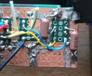
Additionally the ones crossed out in yellow i imagined would be good to remove to isolate the output from the "rear" since they seem to connect to the caps?
So other than that original wiring picture from the last post seems about right?
Once you get the caps out, you can see if anything else is connected to the RCA jacks.
The AVCC wiring drawing you posted looked okay, given a quick cursory check. However, connection isn't the only consideration. Layout is very important too. It isn't shown on a schematic, but its important to do it reasonably well for good results. I would suggest you look at how the opamp and other components are wired up in the pics I posted of my AVCC board. If you can't find the pics, maybe we can help look around for them.
Ooh, those 100k and 47k resistors right next to the caps? Hmm then i dont need to even wire the output at the caps, i can do it at those resistors (once they're removed).Once you get the caps out, you can see if anything else is connected to the RCA jacks.
Great! The I/V stage wiring too?The AVCC wiring drawing you posted looked okay, given a quick cursory check.
However, connection isn't the only consideration. Layout is very important too. It isn't shown on a schematic, but its important to do it reasonably well for good results. I would suggest you look at how the opamp and other components are wired up in the pics I posted of my AVCC board. If you can't find the pics, maybe we can help look around for them.
Thanks for your help. I believe this is the post you're reffering to right?
I have also found this post that will help me make the layout for the AVCC.
For now i still have to wait for the perf board, couldnt find one in that store i linked previously.
Regards
The I/V stage wiring too?
If you linked to some picture you have of output stage interconnections, I think I must have missed that.
For the output stage, there are some detailed pics of my layout in the output stage instructions zip file I linked to.
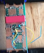
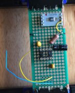
Some other pics of AVCC board and Vref divider during construction below. You should be able to look at both sides and figure out what you are looking at in terms of the layout plan from the schematic. (First and last pics are upside down relative to how they mount to the bottom of the dac board ground plane that would be below when the two were attached together, sorry if hard to visualize that way. To put it another way, the pics are shown right side up as they would be seen once attached to the dac board, and when the dac board is also placed right side up.) Last pic just shows the Vref divider part of the circuit over at the right side as it was being laid out. In the first pic, the two wires in the middle sticking out into space unattached on one end are the outputs that get soldered to the bottom of the AVCC cap vias on the bottom of the dac board.
The idea is to get the decoupling caps right at the opamp power pins, keep the analog inputs separate from the outputs, keep one channel wiring not too close to the other channel wiring, try to keep wiring short and direct, etc. Lots of things to think about when laying out a circuit.
Attachments
Last edited:
Help. my ak4137 does not see usb amanero. playback starts only if you change the filter. nor does the frequency of the incoming signal appear. usb is connected to the computer. drivers installed for amanero
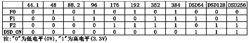
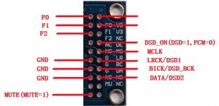
The signals are connected to ak4137: data / bclk / lrck / mclk / dsdon / grd. maybe mclk is superfluous here? since only data / bclk / lrck / grd is connected to es9038. everything works without problems.
also when connecting amanero to ak4137 does not play dsd files. foobar is configured. if you connect amanero to es9038 directly - then there is no pro
USB to AK4137 requires: DATA, BCLK (sometimes called BICK), LRCK (sometimes called WCK or FSCK), DSD_ON (sometimes DE), FO, F1, F2, MUTE, and GND. There should be one ground for each signal wire. If using ribbon cable as recommended, every other wire should be a ground. The ground wires should be individually connected to ground pins if possible, one ground pin per ground wire at each end of the ribbon cable. The most important signals to have an associated dedicated ground wire are the I2S signals: DATA, BLCK, LRCK.
It is strongly recommended to use gold plated pin connectors for AK4137 outputs and for dac board I2S inputs. Either gold or solder, but not nickel or tin plated connectors. That is to help minimize jitter.
Some diagrams below showing where the AK4137 board would expect the input signals as listed above. The two unlabeled red lines at the top right in the middle diagram below are +3.3v outputs from the USB board. They should not be connected to anything on AK4137. No MCLK is needed from the USB board.
NOTE: As explained before, no Chinese XMOS or Amanero board supports Native DSD since it takes paid ASIO drivers. DoP DSD can pass through Windows if Windows Sound Engine doesn't do any DSP on the digital audio stream, something that cannot be assured. Also, AK4137 does not understand DoP format so DoP would have to be played with the USB baord directly connected to the dac board I2S inputs.
Attachments

Last edited:
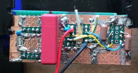
Oh sorry, here is the pic in question from post #5037 Imgur: The magic of the Internet (i made it before you elucidated i can connect the output to pads of resistors (or caps) near the output caps on the board to use the original outputs)If you linked to some picture you have of output stage interconnections, I think I must have missed that.
Thank you, those pictures are pretty good, i cross referenced with the diagram and it makes a lot of sense i see where everything is and keeping everything tight and efficient.Some other pics of AVCC board and Vref divider during construction below. You should be able to look at both sides and figure out what you are looking at in terms of the layout plan from the schematic. (First and last pics are upside down relative to how they mount to the bottom of the dac board ground plane that would be below when the two were attached together, sorry if hard to visualize that way. To put it another way, the pics are shown right side up as they would be seen once attached to the dac board, and when the dac board is also placed right side up.) Last pic just shows the Vref divider part of the circuit over at the right side as it was being laid out. In the first pic, the two wires in the middle sticking out into space unattached on one end are the outputs that get soldered to the bottom of the AVCC cap vias on the bottom of the dac board.
Last edited:
Oh sorry, here is the pic in question from post #5037
You don't show the opamp decoupling caps. There is no cap implemented across the inverting inputs of the I/V opamps, it was considered and rejected. There is a schematic in the output stage zip file that shows all the components.
Whether you decide to use the components shown in the BOM or the other schematic parts values (such as used by Topping), it matters that the parts are good quality. Use NPO or C0G for any caps in the audio path. Bypass ceramic caps are X7R, do not use NPO/C0G for those. Resistors are 0.1% or better if at all possible. If not possible, distortion will probably be higher than it would be with the correct parts. If only 1% resistors are available, one could measure the actual values and try to match them symmetrically for the I/V opamp and the differential summing opamp for each channel. The idea is to help cancel out common-mode distortion which will work best if the resistor values are exactly matched. Doesn't matter so much if the two stereo channels are exactly the same, matching matters the most for the resistors and caps within each individual channel.
Building the output stage with the components installed as shown is a very tight fit, but doable if planned out correctly. Decide which wires and components will go in first and assemble them first on the bottom layer nearest the socket and ground plane. Power wiring and bypass caps need to be considered there. Then plan to install the next components being sure to leave room for any remaining components. Probably easier to do if we had used SMD parts since they are easier to fit in a small space, but some people would only consider building with through-hole parts. Would have preferred to build using SurfBoards to mount SMD parts: SURFBOARDS FOR I.C.s Model 9081 Surface Mount Breadboard
Last edited:
Oh, you're right its not in this schematic. So onMrSlim's post, the capacitors C1, C6, C7 and C12 should be removed? Okay, thanks!You don't show the opamp decoupling caps. There is no cap implemented across the inverting inputs of the I/V opamps, it was considered and rejected.
I took the schematic from your .rar with the word document with pictures of the output stage, (the one you linked a few posts ago, from the dropbox).There is a schematic in the output stage zip file that shows all the components.
Oh, i didn't consider this 😱. Thank you for telling me, this is an important consideration. I know ebay has a lot of fake opamps, but what do you think my chance of getting fake 0.1% resistors is? Otherwise i just might have to match them with a multimeter with not much decimal points.Whether you decide to use the components shown in the BOM or the other schematic parts values (such as used by Topping), it matters that the parts are good quality. Use NPO or C0G for any caps in the audio path. Bypass ceramic caps are X7R, do not use NPO/C0G for those. Resistors are 0.1% or better if at all possible. If not possible, distortion will probably be higher than it would be with the correct parts. If only 1% resistors are available, one could measure the actual values and try to match them symmetrically for the I/V opamp and the differential summing opamp for each channel. The idea is to help cancel out common-mode distortion which will work best if the resistor values are exactly matched. Doesn't matter so much if the two stereo channels are exactly the same, matching matters the most for the resistors and caps within each individual channel.
I will try to hold to the Quality values specified in the BOM v0.3.
Luckily the local store has the X7S 100nF. Its not the 100V version but it should do i suppose.
I've done some SMD in the past, but i think ill do trough-hole as well. The layout on the picture was more of an "exploded view", i'll try to get it as tight as possible and cable runs as short as possible, just like you did.Building the output stage with the components installed as shown is a very tight fit, but doable if planned out correctly. Decide which wires and components will go in first and assemble them first on the bottom layer nearest the socket and ground plane. Power wiring and bypass caps need to be considered there. Then plan to install the next components being sure to leave room for any remaining components. Probably easier to do if we had used SMD parts since they are easier to fit in a small space, but some people would only consider building with through-hole parts. Would have preferred to build using SurfBoards to mount SMD parts: SURFBOARDS FOR I.C.s Model 9081 Surface Mount Breadboard
Last edited:
the capacitors C1, C6, C7 and C12 should be removed?
No! Those need to stay.
I was referring to a cap with no value connected across the + and - dac outputs before going into the I/V opamps. No cap is used there, that's why it has no value on the schematic you used.
I took the schematic from your .rar with the word document with pictures of the output stage, (the one you linked a few posts ago, from the dropbox).
Understood. It does not show opamp power pin decoupling caps. I included it only to help understand what was shown in some pics. That's what the color coding is for.
Otherwise i just might have to match them with a multimeter with not much decimal points.
In addition to tolerance/matching considerations, through-resistors should be metal film types for lowest distortion. For example: https://www.vishay.com/docs/31027/cmfmil.pdf
If using SMD resistors, we would use low distortion thin film resistors, likely from Susumu or Vishay.
Whoops, didnt even see that one! Yeah, thanks for telling me. Seems like MrSlim's post #3003 is the go-to schematic, i will build from there, parts are on the way. As you say, the schematic i picked was just to show the wiring on the perf board images.No! Those need to stay.
I was referring to a cap with no value connected across the + and - dac outputs before going into the I/V opamps. No cap is used there, that's why it has no value on the schematic you used.
I got it, it was a decent help to correlate what was going on the pictures with the schematic. 🙂Understood. It does not show opamp power pin decoupling caps. I included it only to help understand what was shown in some pics. That's what the color coding is for.
I saw you used some Vishays on your board, and also read it on the ess component selection pdf, so i figured as much. However as you might guess yep, cant find these here.In addition to tolerance/matching considerations, through-resistors should be metal film types for lowest distortion. For example: https://www.vishay.com/docs/31027/cmfmil.pdf
If using SMD resistors, we would use low distortion thin film resistors, likely from Susumu or Vishay.
Maybe if i order from ebay, i dont know if they're faking resistors these days.
P.S sorry for all the questions, sometimes i get confused, but i have learned a lot from your help. At least we bumped the thread 10 pages..
Last edited:
Page 15 of the TI vref reference design manual shows a chart with different values of caps on the low pass filter cap on the output.
on the current AVCC design it is 10uF tantalum.
Do you think further improvements could be made to the noise attenuation with a larger (say 47uf) tantalum as the chart implies?
on the current AVCC design it is 10uF tantalum.
Do you think further improvements could be made to the noise attenuation with a larger (say 47uf) tantalum as the chart implies?
Page 15 of the TI vref reference design manual shows a chart with different values of caps on the low pass filter cap on the output.
on the current AVCC design it is 10uF tantalum.
Do you think further improvements could be made to the noise attenuation with a larger (say 47uf) tantalum as the chart implies?
Aluminum Electrolytics should be fine. Tantalum has some different properties and is much more non-linear as a function of voltage. In this particular case the difference may not matter since the voltage should be quite stable. You can try 47uf if you want. The 10k resistor works with the cap to make a simple low-pass filter. Increasing the cap value will lower the corner frequency. No harm in doing it, although it will make the filter output voltage take a little longer to settle when the circuit is first powered up. ESS used a 10uf cap with their example opamp AVCC supply, but there is no magic number. 10uf or 47uf, either one is probably fine. Of course, the amount of filtering needed depends on how noisy your voltage reference is and how much noise you can tolerate, but LTC665 or LT304x are both very low noise to begin with so no worries.
Got it, it makes sense. If i had a scope i would try it just to measure, but im certain this difference will not be heard (or at least very difficult), so as you say doesnt matter much for our already low noise supply. Thanks for the replyAluminum Electrolytics should be fine. Tantalum has some different properties and is much more non-linear as a function of voltage. In this particular case the difference may not matter since the voltage should be quite stable. You can try 47uf if you want. The 10k resistor works with the cap to make a simple low-pass filter. Increasing the cap value will lower the corner frequency. No harm in doing it, although it will make the output value take a little longer to settle when the circuit is first powered up. ESS used a 10uf cap with their example opamp AVCC supply, but there is no magic number. 10uf or 47uf, either one is probably fine. Of course, the amount of filtering needed depends on how noisy your voltage reference is and how much noise you can tolerate, but LTC665 or LT304x are both very low noise to begin with so no worries.

P.S sorry for all the questions, sometimes i get confused, but i have learned a lot from your help. At least we bumped the thread 10 pages..
Happy to help, so long as you are interested in learning its all good.
However, if you are serious about learning more electronics then you will need to study some books (happy to make some recommendations). If you just want to know enough to mod a dac, that's fine too.
Sort of looks like you have been searching around for some information since you turned up the TI app note. Have you read the book, The Art of Electronics, yet? Well worth your time if you want more than just app note type things.
I've been chipping away at Electromagnetic Compatibility Engineering, its quite long. Now i have an even longer one to read! 😱Happy to help, so long as you are interested in learning its all good.
However, if you are serious about learning more electronics then you will need to study some books (happy to make some recommendations). If you just want to know enough to mod a dac, that's fine too.
Sort of looks like you have been searching around for some information since you turned up the TI app note. Have you read the book, The Art of Electronics, yet? Well worth your time if you want more than just app note type things.
My schedule might get real busy in a moment with work so i'm just using the time i have now as best i can. Have to expand my horizons, learn some EE you know? So much things im going to miss out on knowing if i dont try at it.
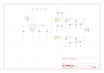
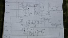
Also, i've drawn a technical drawing from MrSlim's schematic.
I apologize if its a bit messy (i admit, space management wasnt the best), but maybe it helps someone with the modding.
(if you have the time or will, can you tell if something is wrong so people dont look at it in case there's a mistake)
P.S, the R50-53 resistors for the balanced output are 0 ohm, i.e deprecated?
Higher res link (imgur)
Attachments
Last edited:
- Home
- Source & Line
- Digital Line Level
- ES9038Q2M Board