Yes, I was just going to ask Chris if these were mixed signal systems he was talking about as I suspected not - GHz speeds are associated with digital only communication so the noise budget is concerned with not causing bit errors (BER) Edit: Ok, I see now he mentioned they are mixed signal boards - can I ask what the analog part does?
This is a far different consideration than the possible effect of this noise on the associated analog parts & why I say it is generally ignored - people tend to have expertise in digital or in analog - mixed signal experts are not too abundant
This is a far different consideration than the possible effect of this noise on the associated analog parts & why I say it is generally ignored - people tend to have expertise in digital or in analog - mixed signal experts are not too abundant
Last edited:
Could you make a drawing? I don't understand what you mean from this description.
Yes, I really need to draw this up to help explain, but your giving the same encoded energy state to the RTZ "Blanking period" as you are to Data Zero - so your encoding the RTZ blanking period as if it was part of the signal rather then its true purpose of insuring that the energy contribution of each pulse is independent of the previous / next state.
The DAC arrangement you use with the complementary signals from the FF and using the 02 and 08 gates would work correctly here.
WRT the best 74AC logic, TI have an AC logic family where they rearrange the pinning and moved the power pins to the center of the device package (this should have been adopted as the standard pinning arrangement IMO) - before TinyLogic UHS was available these where the best logic family for our Sudo Digital / Analogue applications.
The 74AC11074 is still the best choice when you need a truly balanced design as the modulation on the power pins is then balanced and is later cancelled (factoring the limitations of Common Mode rejection) in the Analogue Diff stage (as long as the input data to the pair of FF is also symmetrical)...
http://www.ti.com/product/74AC11074
Last edited:
I'd like to just quickly mention that I see many designs where only a single filter capacitor is strapped between the differential outputs of the LPF - this is EXTREMELY bad practice as this can ONLY filter the differential noise products - offering zero filtering to common mode noise signals. This single capacitor strapped between the Diff pairs should be replaced with two capacitors - one on each Diff output to Ground (the capacitors will need to be x2 in capacitance value of the original single capacitor to maintain the same filter response as they are in effect in series with each other).
I see this arrangement on so many manufacturers datasheets where they should really know better...
I see this arrangement on so many manufacturers datasheets where they should really know better...
Yes, I really need to draw this up to help explain, but your giving the same encoded energy state to the RTZ "Blanking period" as you are to Data Zero - so your encoding the RTZ blanking period as if it was part of the signal rather then its true purpose of insuring that the energy contribution of each pulse is independent of the previous / next state.
The DAC arrangement you use with the complementary signals from the FF and using the 02 and 08 gates would work correctly here.
WRT the best 74AC logic, TI have an AC logic family where they rearrange the pinning and moved the power pins to the center of the device package (this should have been adopted as the standard pinning arrangement IMO) - before TinyLogic UHS was available these where the best logic family for our Sudo Digital / Analogue applications.
The 74AC11074 is still the best choice when you need a truly balanced design as the modulation on the power pins is then balanced and is later cancelled (factoring the limitations of Common Mode rejection) in the Analogue Diff stage (as long as the input data is also symmetrical)...
http://www.ti.com/product/74AC11074
Very nice feature with clk/data removed from the two Q outs . I agree, all FF should have this configuration. Unfortunately the 74AUC1G74, does not have this feature, but it is faster.
I cannot find any data on the fall and rise time difference for the AUC but the AC110 has that, on the other hand the switching characteristic for the AUC is better, due to its higher speed, I suppose.
Thanks Koldby,
So is the Hazard circuit on page 171 valid? Seems 6n8 isn't such a large cap? I know I will need one 74AUC1G per channel as per your schematic.
So John, I think I understand what you are saying regarding the capacitors on the output they would each be dbl the capacitance connected in series across q-q' and also to ground in the middle?
Thanks
So John, I think I understand what you are saying regarding the capacitors on the output they would each be dbl the capacitance connected in series across q-q' and also to ground in the middle?
Yes, Correct
")
Thanks John,
On the Hazard circuit p171 there is also a 47n cap in front of the 220R resistors in that circuit, same treatment for it?
Yes best for both positions.
This capacitor is what I was warning about...Do not place that at all as it loads the FF too much, regardless if it is placed between q and q' or the double valueThanks John,
On the Hazard circuit p171 there is also a 47n cap in front of the 220R resistors in that circuit, same treatment for it?
to ground.If you want 12 dB/oct use R-L-C or use a R-C-R-C configuration..
Be sure not to load the FF too much.
By the way Koldby what does it sound like ?? You've had time to listen ? I'm perfectly happy to build your simpler R-C version
Sorry I have been busy with a lot of other things, so no progress here.
I will report, though , as soon as I have new results..
Yes, I really need to draw this up to help explain, but your giving the same encoded energy state to the RTZ "Blanking period" as you are to Data Zero - so your encoding the RTZ blanking period as if it was part of the signal rather then its true purpose of insuring that the energy contribution of each pulse is independent of the previous / next state.
The DAC arrangement you use with the complementary signals from the FF and using the 02 and 08 gates would work correctly here.
Ah, OK. I think you mean that you would prefer a three-level DAC, with an intermediate level that's only used for the blanking period, as you call it.
Not taking into account clock jitter, when you subtract the waveforms of the three-level and the two-level version, you will see that the difference is a simple square wave at the bit rate. The low-pass filter that suppresses the out-of-band quantization noise will also filter off this square wave.
Taking into account clock jitter, I suspect the three-level version is 3 dB less sensitive to (white) clock jitter. I would have to write out the equations properly to be sure, but the steps in the output waveform are halved, which helps by 6 dB, and the average number of transitions is doubled, which presumably makes one lose 3 dB again.
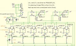
If you want to design RTZ signal in FPGA, "clock gate" is usually inhibited because the clock is dedicated to drive clock input only to ensure low jitter and skew. 100MHz clock with more than 1000 fanouts is ordinary in FPGA design. Instead, double clock rate or DDR FF is used to make RTZ. Double clock (2x100MHz) ends up high power consumption. DDR FF is better for RTZ like the attached pic since the double rate is local.
BTW, I'm now designing DA converter(no DAC chip) for 1bit DSM. No DAC topology usually has 0 PSRR, which is the disadvantage of no DAC. I tried ECL logic conversion to have some PSRR before. I wasn't able to have a good result because it had only one tap, and the driver was poor. My current design has 24 taps and a powerful driver, e.g., SSTL15 designed for DDR3(up to 800MHz). My PCM to DSM conversion implemented by FPGA is already finished. The rest to the goal is ideal PA conversion, I would say Pulse to Analog, in 1bit DSM. How about the attached pic?
Thanks for sharing.
Do you know maybe some JFET type that could be used as switch? For network switch, like BJT You use?Thanks for sharing.
This is a differential ECL. One tap(T1 and T13) is the current switch(T1) and current source(T13). If you remove T13 and connect the collector and the emitter, you have typical ECL buffer with a differential input. I'm sure active current source is better than passive one constructed by one register, though I need to do some trial and error with the real PCB.
T1 is non-saturated current switch driven by SSTL15. In 1 state, LP_0 is 0.75+0.35=1.1V, LN_0 is 0.75-0.35=0.4V. In 0 state, LP_0 is 0.75-0.35=0.4V, LN_0 is 0.75+0.35=1.1V. The difference(0.7V) is enough to turn on or off the two transistors of T1. The transition time is minimal (0.2nS) because SSTL15 is up to 800MHz capacity. The disadvantage of ECL is the difference between turn on and off. Turn on is active while turn off is passive. I don't know how much it dominates the performance. But you are almost free from disturbance caused by digital switching, though terminated transfer(75 ohms), small voltage swing(0.7V) and non-saturation(constant current) are in favor for you.
FPGA(xc6slx9 in QFT144) has 25 differential SSTL15 drivers with the internal 75-ohm resistor. That's why you need two FPGAs for stereo DAC(I need 24 drivers for one channel). But two chips have the advantages, where PCB layout is easier than one large FPGA, and DIY friendly package(QFP) is available. One FPGA for one channel isn't a bad design.
As to JFET, I know high-speed analog switches supplied by AD and have some experience with them before. They are not discrete part but monolithic one for me, which means fine adjustment isn't available. I have no experience with a single JFET for high-speed switching. It's easy for me to use a transistor for "pulse" to analog conversion with FPGA which have the job in the digital domain, i.e., PCM to DSD conversion, pulse width adjustment for compensating the difference between turn on and off and optimum usage of 24 taps.
Attachments
Koldby, please try to explore another digital isolator IC. Somehow I have better results with ADUM1100, single isolator, against mostly used all-in-one ISO7640?
And I would double, repeat, F-F to complete one (full) cycle of MCK clocking?
...
What about some listening impressions?
And I would double, repeat, F-F to complete one (full) cycle of MCK clocking?
...
What about some listening impressions?
- Home
- Source & Line
- Digital Line Level
- The Best DAC is no DAC