^ Agree with this - digital is a concept that has to be realised in integrated circuits that operate according to the laws of physics - no such thing as instant 1 & 0s - there's all sorts of issues that are already known in the world of analogue electronics, just at a lower & faster level. These issues are often ignored as they are considered too low a level to be audible.
As you point out modulation issues, particularly in the ground plane seem to be one of the main offenders in all of this
There was an interesting question asked earlier by Koldby - about the necessary averaging used in FFTs missing the dynamic noise modulation aspects & this might be masking what could be obvious if some other sensitive measurement technique could be used which didn't involve this masking by averaging.
Any thoughts?
Well, which part is in your eyes the one with the lowest jitter (and causes more delay): is it directly at the output of the flip flop or the output of the added gates behind that flip flop? This seems logical because with the RTZ circuit after the FF you'd have to add both jitters (FF + RTZ) to the signal when having the FF as the last part means 1 less jitter added.
I also suspect I don't really get what you mean because this is so obvious.
As far as data or clock feedthrough go: I suspect that's one of the reasons why source jitter before a FF still can be measured even when setup times are met.
I've drawn a picture to show what I mean. The input data change at the falling clock edge in the drawing, but any position that meets the set-up and hold time requirements would be just as good.
For clarity, I assume a relatively slow flip-flop with about a quarter of a clock cycle of delay and a fast NOR gate. By inspecting the schematic and the timing diagram, you will see that the output transitions of the NOR (node Y) are caused by the clock transitions. The flip-flop output (node A) gates the clock pulses, but does not affect the delay from clock to node Y as long as certain timing constraints are met (*).
Hence, small variations in the flip-flop's delay (flip-flop jitter) don't affect the output. Only the NOR gate's jitter and the clock jitter reach node Y.
(*): That is, the delay must be more than the difference in propagation delays between the NOR gate inputs, and less than the time that the clock pulse is high minus the difference in propagation delays between the NOR gate inputs. In fact, because of possible pattern sensitivity of the NOR gate's delay, it is probably safest if the flip-flop's delay is greater than or equal to the NOR gate's delay and smaller than or equal to the time that the clock is high minus the NOR gate's delay.
Attachments

This still doesn't make any sense to me. The way logic gates, latches and flip-flops can worsen jitter is by small random variations of their delay (due to noise, supply ripple or whatever). Hence, any delay that is not in the path from clock to output does not worsen the jitter.
If you design your RTZ circuit properly, the clock and the delay of the logic gate determine when the output switches. The data coming from the flip-flop switch at moments when the gate is not sensitive anyway, because the other input determines its output level.
I've drawn a picture to show what I mean. The input data change at the falling clock edge in the drawing, but any position that meets the set-up and hold time requirements would be just as good.
For clarity, I assume a relatively slow flip-flop with about a quarter of a clock cycle of delay and a fast NOR gate. By inspecting the schematic and the timing diagram, you will see that the output transitions of the NOR (node Y) are caused by the clock transitions. The flip-flop output (node A) gates the clock pulses, but does not affect the delay from clock to node Y as long as certain timing constraints are met (*).
Hence, small variations in the flip-flop's delay (flip-flop jitter) don't affect the output. Only the NOR gate's jitter and the clock jitter reach node Y.
(*): That is, the delay must be more than the difference in propagation delays between the NOR gate inputs, and less than the time that the clock pulse is high minus the difference in propagation delays between the NOR gate inputs. In fact, because of possible pattern sensitivity of the NOR gate's delay, it is probably safest if the flip-flop's delay is greater than or equal to the NOR gate's delay and smaller than or equal to the time that the clock is high minus the NOR gate's delay.
I get it now. Because you are solely depending on the clock signal and assume a NOR can be found (or many are?) that have very low jitter it works as described. Clever way of making use of the delay
Yet this solution makes the circuit depending on the falling edge as well and by that you need a solution that ensures stable duty cycle and the pro of the need for a lower clock is out the window because you gain double the jitter by the addition of jitter of the falling edge.
In the end I can't see it performs better or worse than a FF at double the clock speed, but good to see "there's many ways to get to Rome", as they say ;-)
Thanks for clearing that up Marcel!
RTZ indeed has the disadvantage of increased sensitivity to jitter and when you implement it like I do, sensitivity to duty cycle variations.
You can largely get rid of the increased sensitivity to jitter and the duty cycle dependence by making a FIRDAC with an even number of taps working on opposite edges, always using equal weights for a pair of unit DACs. Simplest example: one RTZ DAC that produces a pulse when clock = 0 and one that produces a pulse when clock = 1, outputs added with equal weights.
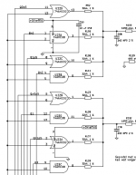
Attached is a fragment of a schematic for a four-tap differential FIRDAC. Note that all the logic gates get the same clock. The corresponding flip-flops (not in the picture) get opposite clocks. The full schematic is here: 74AHC02 and 74AHC08 DAC with 97 dB(A) dynamic range
(I used fairly fast flip-flops because at the 27 MHz clock rate, a 74HC74 could have a delay of more than half the clock cycle. The CD74AC74 seemed nice because it has a larger guaranteed minimum delay than most fast flip-flops.)
You can largely get rid of the increased sensitivity to jitter and the duty cycle dependence by making a FIRDAC with an even number of taps working on opposite edges, always using equal weights for a pair of unit DACs. Simplest example: one RTZ DAC that produces a pulse when clock = 0 and one that produces a pulse when clock = 1, outputs added with equal weights.
Attached is a fragment of a schematic for a four-tap differential FIRDAC. Note that all the logic gates get the same clock. The corresponding flip-flops (not in the picture) get opposite clocks. The full schematic is here: 74AHC02 and 74AHC08 DAC with 97 dB(A) dynamic range
(I used fairly fast flip-flops because at the 27 MHz clock rate, a 74HC74 could have a delay of more than half the clock cycle. The CD74AC74 seemed nice because it has a larger guaranteed minimum delay than most fast flip-flops.)
Attachments
I've drawn a picture to show what I mean. The input data change at the falling clock edge in the drawing, but any position that meets the set-up and hold time requirements would be just as good.
For clarity, I assume a relatively slow flip-flop with about a quarter of a clock cycle of delay and a fast NOR gate. By inspecting the schematic and the timing diagram, you will see that the output transitions of the NOR (node Y) are caused by the clock transitions. The flip-flop output (node A) gates the clock pulses, but does not affect the delay from clock to node Y as long as certain timing constraints are met (*).
Hence, small variations in the flip-flop's delay (flip-flop jitter) don't affect the output. Only the NOR gate's jitter and the clock jitter reach node Y.
(*): That is, the delay must be more than the difference in propagation delays between the NOR gate inputs, and less than the time that the clock pulse is high minus the difference in propagation delays between the NOR gate inputs. In fact, because of possible pattern sensitivity of the NOR gate's delay, it is probably safest if the flip-flop's delay is greater than or equal to the NOR gate's delay and smaller than or equal to the time that the clock is high minus the NOR gate's delay.
Yes, I understood this, but the reality is that the typical propagation delay of a fast FF is 2.2nS (with a min of 800pS) - in fact I find typical values around 1.5nS these days with the NC7SZ74 I use...
Your timing diagrams show a totally unrealistic propagation delay unless the circuits operating in the GHz region (I know you say you use a slow FF, but its not the case of todays FF)...
The danger here is that your NOR Flips on one input and changes state via the second input so both inputs contribute to the output Jitter (point I'm sure your aware off as you used a FF in your simulations with unrealistic PD)- Maybe OK for DIY build, but its not recommended to design a production circuit like this as one could not guarantee stable operation in all conditions, the point is relatching the output removes this uncertainty.
When your operating logic with such tight timing conditions (input transitions occurring close to each in time) the output switching edges are not so well defined as the outputs are in an unstable equilibrium or metastable state - this is seen as worst phase noise.
I don't mean to use the term metastable state as used with a FF where the output could finally end up in an unknown state until it finally happens, but that the output impedance of the switching edge could be somewhere in between states for longer period or could briefly oscillate between states - this will be seen as worst then expected phase noise.
There is such a variance in DIY Builds that its better to avoid asynchronous operation unless delays where introduced into the circuit that would guarantee to avoid such conditions.
With such tight switching periods you also have the issue of Ground bounce, your NOR gate is operating during a period where the Ground is still bouncing around from the FF operation...
Maybe I'm just being too perfect, but I can guarantee that you will not reach measured high performance operating like this (and for sure why so many projects have such relatively poor noise performance). With care its possible to reach Dynamic range figures of 130dB+ (DSD256) but not working like this...
Please understand I'm not criticizing you - its all about learning, I've been designing discrete DAC's now for over 30 years, some audio IC's and also discrete designs... I know from hard learnt experience whats required to achieve high measured performance.
Last edited:
The timing diagrams just illustrate the concept and have no time scale, so how on Earth do you know whether they are realistic and why would it matter in the first place?
^ Agree with this - digital is a concept that has to be realised in integrated circuits that operate according to the laws of physics - no such thing as instant 1 & 0s - there's all sorts of issues that are already known in the world of analogue electronics, just at a lower & faster level. These issues are often ignored as they are considered too low a level to be audible.
As you point out modulation issues, particularly in the ground plane seem to be one of the main offenders in all of this
There was an interesting question asked earlier by Koldby - about the necessary averaging used in FFTs missing the dynamic noise modulation aspects & this might be masking what could be obvious if some other sensitive measurement technique could be used which didn't involve this masking by averaging.
Any thoughts?
You can try using a mix between many or no averaging, changing frequencies, levels all the way up to multitone and mixed signals etc.
It might show stuff you didn't know were there, and it makes a good map of where your boundaries are, but it's time consuming as most measurements are.
What makes designing a no DAC so challenging is that you can pick a sine, set the level and the frequency and discover a pattern of it's distortion products.
Now change the frequency or level and the pattern changes.
Change the bit depth of the pcm source, the modulator and/or algorithm and again it all changes, or maybe just the noise floor that does. Now change the arrangement of the wiring of the power supply on the proto board and things shift yet again. Is it better or different?
And sooner or later you're gonna be on crossroads and you have to choose if the goal is to achieve the highest dynamic range or the lowest distortion? Just for instance.
What to make of this stuff?
There's so much going on that at these measurement levels you're bound to find something and you have to make meaning of it.
I don't think there's much we can't measure but knowing the meaning or importance of what the measurement shows can only be interpreted well if you know everything there is to know. Nobody does so there's alway more knowledge (or meaning) to gain.
It just shows your level of expertise, it's you who is on the edge out there discovering Star Trek style. Enjoy!
RTZ indeed has the disadvantage of increased sensitivity to jitter and when you implement it like I do, sensitivity to duty cycle variations.
You can largely get rid of the increased sensitivity to jitter and the duty cycle dependence by making a FIRDAC with an even number of taps working on opposite edges, always using equal weights for a pair of unit DACs. Simplest example: one RTZ DAC that produces a pulse when clock = 0 and one that produces a pulse when clock = 1, outputs added with equal weights.
Attached is a fragment of a schematic for a four-tap differential FIRDAC. Note that all the logic gates get the same clock. The corresponding flip-flops (not in the picture) get opposite clocks. The full schematic is here: 74AHC02 and 74AHC08 DAC with 97 dB(A) dynamic range
(I used fairly fast flip-flops because at the 27 MHz clock rate, a 74HC74 could have a delay of more than half the clock cycle. The CD74AC74 seemed nice because it has a larger guaranteed minimum delay than most fast flip-flops.)
I wanted to say that with just a NOR circuit in the ADC you are not correctly encoding "DSD data" - this in itself will introduce an error - the Zero Data and RTZ period are Zero... your complementary NOR / AND approach correctly decodes the data (but with my concerns surrounding the phase noise).
If your OK, I'd rearrange your ADC Front-end and DAC section to be truly balanced 🙂 it be interesting to see how your NS then perform...
74AC logic is a great logic family - I'm sure just swapping the HC logic in your designs with AC will yield a SNR / THD improvement - but I strongly recommend that you try UHS TinyLogic which is the best logic family I've worked with todate (better performance then even PECL).
Koldby,
You have me convinced to try the 74AUC1G, could it be subbed for the 74 part in the page 171 Hazzard schematic from earlier in this thread? Using his output filter?
Thanks
You have me convinced to try the 74AUC1G, could it be subbed for the 74 part in the page 171 Hazzard schematic from earlier in this thread? Using his output filter?
Thanks
Last edited:
Thank you - engage the warp drive 😀You can try using a mix between many or no averaging, changing frequencies, levels all the way up to multitone and mixed signals etc.
It might show stuff you didn't know were there, and it makes a good map of where your boundaries are, but it's time consuming as most measurements are.
What makes designing a no DAC so challenging is that you can pick a sine, set the level and the frequency and discover a pattern of it's distortion products.
Now change the frequency or level and the pattern changes.
Change the bit depth of the pcm source, the modulator and/or algorithm and again it all changes, or maybe just the noise floor that does. Now change the arrangement of the wiring of the power supply on the proto board and things shift yet again. Is it better or different?
And sooner or later you're gonna be on crossroads and you have to choose if the goal is to achieve the highest dynamic range or the lowest distortion? Just for instance.
What to make of this stuff?
There's so much going on that at these measurement levels you're bound to find something and you have to make meaning of it.
I don't think there's much we can't measure but knowing the meaning or importance of what the measurement shows can only be interpreted well if you know everything there is to know. Nobody does so there's alway more knowledge (or meaning) to gain.
It just shows your level of expertise, it's you who is on the edge out there discovering Star Trek style. Enjoy!
I wanted to say that with just a NOR circuit in the ADC you are not correctly encoding "DSD data" - this in itself will introduce an error - the Zero Data and RTZ period are Zero... your complementary NOR / AND approach correctly decodes the data (but with my concerns surrounding the phase noise).
Could you make a drawing? I don't understand what you mean from this description.
If your OK, I'd rearrange your ADC Front-end and DAC section to be truly balanced 🙂 it be interesting to see how your NS then perform...
I haven't really got an application for the ADC, so I have no intention of rearranging it. If you or anyone else would want to try a balanced version, you/they can go ahead, of course. The KiCAD database is included in the ADC's thread.
74AC logic is a great logic family - I'm sure just swapping the HC logic in your designs with AC will yield a SNR / THD improvement - but I strongly recommend that you try UHS TinyLogic which is the best logic family I've worked with todate (better performance then even PECL).
I've mainly used AHC logic rather than HC logic. Thanks for recommending UHS TinyLogic!
The timing diagrams just illustrate the concept and have no time scale, so how on Earth do you know whether they are realistic and why would it matter in the first place?
I understand the idea but for the concept to work correctly WITHOUT impacting the phase noise relies upon unrealistic PD delays - delays that in reality with today's fast logic and our DSD clock rates (as I say typical AC / UHS logic PD are in the 1-3ns - this delay does not place the clock conveniently almost 90deg away)...
My point is that the idealized timing diagram its not whats happening with the circuit in reality - and this is the important consideration.
Its clear that we are sadly running around in circles here 🙂
For those who are interested within the next 6 -9 months there will be a sub GBP 400 DAC for sale that has a fully discrete DAC (well the whole design is discrete from PSU's, Clock, DAC and Analogue stage) - the PCB has over 1800 components due to its fully discrete nature - the challenge we face will be the build complexity, so few designs these days are fully discrete - I worry we will have a hard time finding a subcontractor in China who can build such a complex PCB with high yields that will not to impact the build cost too badly. The discrete components are cheap, but the design complexity is much greater so impacting the build cost = so sadly no net advantage in sales cost 🙁 But the Sound quality is in a DIFFERENT league to any of our (Jarek and myself) ESS based designs.
Before these "mass market DACs" are released I'm also nearing completion of a "Private group funded" DAC (funding now long closed) I've been working on this design for far to long and looking forward to the first units. This is also a FULLY discrete but far more advanced design - with the DAC array directly driving the analogue output (Direct Digital 2 Analogue) - without an active Analogue stage 🙂 and yet it still has a typical output impedance that varies between 33ohms at 0dB to 3.5 ohms below -40dB (Output impedance depends on the "Volume level setting" not signal level 🙂 ).
The Array output impedance reduces with volume level hence preserving dynamic range which is dominated by the Arrays thermal noise).
As the volume level is reduce so is the output impedance hence so is the thermal noise contribution of the DAC array. At typical volume level setting of -25dB, the DAC output impedance is 5.25 ohms - plenty low enough considering there is no active analogue stage - a purely passive output stage.
Both designs support DSD input without bit manipulation (no digital domain volume control) - with Gain control performed in the Analogue domain 🙂 so both designs are truly native DSD DAC's - PCM is supported by FPGA modulators.
WRT DiY, one of the challenges to good performance is the requirement for surface mount devices - TinyLogic gates...
That said the Dacopo DAC from 1990 was a basic design and yet still sounds very good IMO - maybe we could work on a DIY board based on its "simple" DAC array. I believe we can achieve say 115dB to 120dB DR.
I guess my only worry would be that before you know it, there will be 10 knock off DIY designs being sold from China!!!
I'd also like to add the THD and DR are not a quality Matrix to sound quality - even a designs with 95dB DR will most likely sound better then most DAC IC's. Whats more important is the level of correlated spuire (non harmonic related spurie components on the noise floor). I've yet to hear a DAC IC sound better then a decent Discrete DAC design.
Last edited:
For those who are interested within the next 6 -9 months there will be a sub GBP 400 DAC for sale that has a fully discrete DAC (well the whole design is discrete from PSU's, Clock, DAC and Analogue stage) - the PCB has over 1800 components due to its fully discrete nature - (...)
I think you better start a new thread about that DAC. There are people on this thread who claim that adding one single flip-flop destroys the magic of the noDAC, and now you come with a PCB with 1800 components? 😉
By the way, did you take intersample overshoots into account for the PCM path? Almost all commercial oversampling DAC chips, interpolation filters and ASRCs hard clip when processing peak sample normalized PCM recordings.
Last edited:
I understand the idea but for the concept to work correctly WITHOUT impacting the phase noise relies upon unrealistic PD delays - delays that in reality with today's fast logic and our DSD clock rates (as I say typical AC / UHS logic PD are in the 1-3ns - this delay does not place the clock conveniently almost 90deg away)...
My point is that the idealized timing diagram its not whats happening with the circuit in reality - and this is the important consideration.
Its clear that we are sadly running around in circles here 🙂
Nor does it need to be 90 degrees away, the actual requirements are in the footnote rather than the diagram. You can use a slower logic family for the flip-flop than for the NOR gate, and the path from the clock to the NOR gate is inherently shorter than the path from the clock via the flip-flop to the NOR gate.
I think you better start a new thread about that DAC. There are people on this thread who claim that adding one single flip-flop destroys the magic of the noDAC, and now you come with a PCB with 1800 components? 😉
Good thinking. As a matter of purist fact: let's start a thread with a wax phonograph cilinder (but I must say mixing waxes destroys the real wax sound) and lets be thorough here: we can loose a few billion gates in our cpu because I like the pure sound of dsd 32 much better than 512 as well as the best sound reproduction of a big band ever was by a full range speaker, mind you this was mono, of course!

Just kidding guys!
P.S
Yes better served in it's own thread for sure. I'm hesitating to say "yes" right away, but really curious nonetheless. I hope to read more about it, if you will of course, before I make a decision. With that pricing it shouldn't be too hard finding a few buyers🙂
That said the Dacopo DAC from 1990 was a basic design and yet still sounds very good IMO - maybe we could work on a DIY board based on its "simple" DAC array. I believe we can achieve say 115dB to 120dB DR.
Very interested!
John "Time is my biggest enemy" W, I second that, but in the practical way as in: not in timing but in quantity of spare time to invest in this.
Oke, could be both of course;-)
It'd be awesome doing something for the DIY community. KISS and a bit of tweak possibilities would imho be the base of the product while still achieving better sound than its competitors. Enough know how and knowledgeable people to work with in this thread.
Let's see if there's enough interest and what the timing budget should be.
Last edited:
Koldby,
You have me convinced to try the 74AUC1G, could it be subbed for the 74 part in the page 171 Hazzard schematic from earlier in this thread? Using his output filter?
Thanks
Yes, but remember that the 74AUC1G74 only contains one FF per chip, so you need two. But it is almost exactly how I do it. I wouldn't place a capacitor this big directly at the output of the FF. It is a very though load for the chip. Remember to only supply it with a 3,3 V cell, it will NOT survive 6V.
^ Agree with this - digital is a concept that has to be realised in integrated circuits that operate according to the laws of physics - no such thing as instant 1 & 0s - there's all sorts of issues that are already known in the world of analogue electronics, just at a lower & faster level. These issues are often ignored as they are considered too low a level to be audible.
As you point out modulation issues, particularly in the ground plane seem to be one of the main offenders in all of this
Any thoughts?
In fact, this is all very well known in high speed digital. Common 74HC or AC single ended CMOS logic is stuff from 30 years ago. Real high speed digital is very demanding and all these effects have been considered, because it is a challenge to operate links at GHz+ speeds over any significant distance, while maintaining low power consumption, noise immunity, and EM compliance.
Modern devices are using LVDS, LVPECL, HSTL/SSTL, HCSL, etc.
I have 10 of these FPGAs on my desk, from this family anyway, I don't have it in front of me to read every number off the package.
5AGXFB7H4F35C4N Intel | Integrated Circuits (ICs) | DigiKey
They are a "mid range" few year old part and have 6Gbps+ transceivers. The boards are mixed signal, 12 layers and full of controlled impedance traces.
So, I would not say they are ignored at all. They may be ignored by audio designers which have a concept of digital stuck somewhere in 1985.
Last edited:
In fact, this is all very well known in high speed digital. Common 74HC or AC single ended CMOS logic is stuff from 30 years ago. Real high speed digital is very demanding and all these effects have been considered, because it is a challenge to operate links at GHz+ speeds over any significant distance, while maintaining low power consumption, noise immunity, and EM compliance.
Modern devices are using LVDS, LVPECL, HSTL/SSTL, HCSL, etc.
I have 10 of these FPGAs on my desk, from this family anyway, I don't have it in front of me to read every number off the package.
5AGXFB7H4F35C4N Intel | Integrated Circuits (ICs) | DigiKey
They are a "mid range" few year old part and have 6Gbps+ transceivers. The boards are mixed signal, 12 layers and full of controlled impedance traces.
So, I would not say they are ignored at all. They may be ignored by audio designers which have a concept of digital stuck somewhere in 1985.
You're absolutely right but partly missing the point. In "real digital" meaning just 1's and 0's, the intrinsic signal quality is meant to stay within certain limits to be sure of the integrity of the calculations that have to be done or to get data get across a certain distance.
In the No-DAC these limits are somewhat different and can best be treated as being an analog signal.
That also holds true for ecl, lvds clock signals.
These need to meet higher standards than "just" digital systems because any change in quantity or quality means a direct impact on the delivered analog performance.
Another way of looking at dsd dacs is to see them as a clock signal that is being manipulated to get low frequency data out of modulation of HF signals.
Jitter requirements, phase noise, amplitude and low power are excellent when cmos is used knowledgable.
- Home
- Source & Line
- Digital Line Level
- The Best DAC is no DAC