DIR9001+PCM1794+OPA1604+OPA1612
I assume datasheet performance because it is once again beyond the capability of my test gear (THD 0,0005%).
🙂
And now I need an amplifier for this, so our little project here was the first to come in to my mind!
I assume datasheet performance because it is once again beyond the capability of my test gear (THD 0,0005%).
🙂
And now I need an amplifier for this, so our little project here was the first to come in to my mind!
Firstly, congrats to AIM65 for the new proto. Looks promising.
Just a quick comment about the ARTA measurements though:
Hi,
Thanks for support !.
About Arta, You're right, I'm sure I'm not doing right :
for now, I've only used it on speaker projects where my only interest was the profile of FR curve, for the Xover; nothing about absolute figures and kpi such as distortion or efficiency.
Now I need to learn the process to do right measurements, there are many tuto and how-to guides, including here, it is just a matter of time.
Chris
Last edited:
DIR9001+PCM1794+OPA1604+OPA1612
I assume datasheet performance because it is once again beyond the capability of my test gear (THD 0,0005%).
🙂
And now I need an amplifier for this, so our little project here was the first to come in to my mind!
Nice TI arrangement !
Is it using 3 bridge rectifiers?, I'm sure for one but not so for the two other in rectangle boxing between caps.
Do you have 2 cap multiplier around the 2 BCP56 ?
Can you post schematics ?
Thanks
Chris
Last edited:
Start by building a dummyload/attenuator (preferably adjustable), which has precisely the same attenuation as you have gain in your amplifier under test. Use hi-power thickfilm resistors, do not use wirewound...
Then you just need to cut your loop and put this amp-dummy combo there between and voila! Not touching any adjustments anywhere you used for making the loopback measurement.
🙂
Edit:
About the DAC, no cap-multipliers. I figured out that the less components at the PSUs the better for noise. So there is 6 simple zener-transistor regulators. I used the lowest possible noise zeners I could find. Simulated perfectly. Low avalance voltage zeners. A red LED had more noise than these. The "new" PLZ-series zeners for example.
3 bridge rectifiers for 2* 5VAC and 2*12VAC voltages to create the needed +3.3VDC, +5,0VDC, +15VDC and -15VDC.
Schematics is pretty much PCM1794 datasheet - except for the I/V-stage gain resistors which are adjusted for my liking.
Last edited:
And now I need an amplifier for this, so our little project here was the first to come in to my mind!
I have some pcb left
I´d guess FauxFrench wouldn´t mind trying them ;-)I have some pcb left
Alternatively we could get more PCBs made (rev2?) when we order our TDA7293-composite-PCBs.
Do you mind sharing your layout? I´d love to see how you routed the feedback loops. We haven´t yet started on our layout.
Do you use Kicad?
Of course once we have the TDA7293-composite you´re invited to try that too.
It is indeed a very pretty layout and a PCB would make it easier to assemble two amplifiers for test, one for Chris (chermann) and one for myself. The problem is that an important amount of the components are of the SMD type and I am equipped almost solely with "through hole" type parts. There is a lot of reason in joensd suggestion but I better learn to use Kicad and make a "through hole" version. palstanturhin seems to be fully skilled in SMD assembly and has better test gear than I.
Last edited:
I have some pcb left
If your PCB is what is in post 644, I am interested. It does not look like a complete disaster. But what joensd said; can we see some more pictures?
I am very picky on PCBs, you see...
🙂
My next PCB order from China is completely free of charge, and I would still like to continue where I left = test the circuit with the booster transistors...
But I am definitely interested in your PCB also!
Do you mind sharing your layout? I´d love to see how you routed the feedback loops.
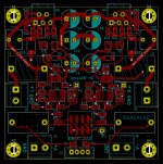
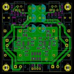
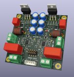
Hi Joensd
Here are some details about the amp pcb. Constructive criticism is welcomed, I still have some questions about some choices I've made, I also have an idea for an improvement. That's the one I've tested after post #665, but with no measurable effect. But let's see if my questions and improvements ideas converge with the ones of this thread readers...
Pictures are: Front - Back - Both then 3D views.
Chris
Attachments

Hi AIM65,Chris
Its a wonderful board. i started one year ago with KICAD but after not using it any more i lost everything in my head.🙄😛
I am not able to criticize your work in making PCB. If you can sum of all your open points what are you planning and points from all other members as a LOP -list of open points then maybe for us its easier to check all of them and can discuss this easier.
just my 2 cents
chris
Thanks a lot; I´ll have a look at it. Can you provide the schematic?Pictures are: Front - Back - Both then 3D views.
It really is a beautiful layout but as much as I appreciate nice looking PCBs, I am in the form follows function camp.
I would have tried to keep both feedback loops as short as possible; no matter what. So I would have moved the opamp near the LM1875.
But that´s me not having much experience with composite layouts, thinking they are terribly sensitive towards any additional inductance introduced.
I also would have tried to use the bottom layer more. Decoupling caps, especially near the chip, can go into the bottom layer, keeping top layer paths cleaner and shorter. Also the bottom is mostly GND-polygon anyway.
I´m not sure I would have put the capacitor/star-GND far away from the supply voltage input. To have the capacitors there might be good but then you better take substantial traces/polygons to that point.
What I definitely get rid of, if you ever make a new layout, is the GND-routing:
You basically created a little loop going from each of the screw-connectors (V+/GND & V-/GND) to the "star-GND". Not only that but the traces are also very thin.
GND is your reference and should be low inductance.
Without a schematic I can´t really trace the GND-routing but it seems you separated high-current-GND-return (speaker) from the rest but again, I think that "loop" and the thin traces rendered that very ineffective.
In theory your circuit and PCB is exactly what I need.
There are things I like and there are things I hate.
What I like most is that it is 2ch and it has only one chipamp/ch!
But then what joensd said...
We need a version v2.0.
V1.0 is good for testing, though...
I try first to spidernet your circuit to my existing PCB and see if I can find some anomalies we need to attend before v2.0 goes in to production...
...what joensd said,
+
this is DIY, you are allowed to bin all manufacturing rules. You are allowed to mix all kinds of components. You are allowed to select the best parts available, be it SMD or TH or what ever, and then mix everything...
Put the connectors where it serves the best audio quality, that is not necessarily at the PCB edge, it may be on the center of it, or just about anywhere on the PCB. The shorter the track the less it interferes with the others.
The power supply leads are twisted together. Keep them tightly together also on the PCB. (-) from the other side and (+) from the other, is a no-no.
Amplifier PCB has 2 grounds; audio GND and power GND. Connect all audio related to the audio GND, that includes the speaker negative. Connect all PSU related to the power GND. Connect these 2 grounds together at one point only. Ideal is the speaker negative terminal(s). On a stereo board the speaker output is likely to be on the middle of the PCB?
You know digital. Think powerGND as your digital and audio GND as your analog.
One said: Copper is FREE! Use it all. That means ground planes and copper pours as large as possible on the power side.
Make audio side super tight and super small = SMD => tiny loop areas.
And: The harder it is to factory make, the better to us DIYers => "they" cant copy our super design. Twist a lead, cut a pin! That would make your copyright.
Hi
thanks for comments, some replies :
I would have tried to keep both feedback loops as short as possible; no matter what. So I would have moved the opamp near the LM1875.
But that´s me not having much experience with composite layouts, thinking they are terribly sensitive towards any additional inductance introduced.
local feedback loop of the two amp are shorts.
I also would have tried to use the bottom layer more. Decoupling caps, especially near the chip, can go into the bottom layer, keeping top layer paths cleaner and shorter. Also, the bottom is mostly GND-polygon anyway.
I´m not sure I would have put the capacitor/star-GND far away from the supply voltage input. To have the capacitors there might be good but then you better take substantial traces/polygons to that point.
What I definitely get rid of, if you ever make a new layout, is the GND-routing:
You basically created a little loop going from each of the screw-connectors (V+/GND & V-/GND) to the "star-GND". Not only that but the traces are also very thin.
Without a schematic I can´t really trace the GND-routing but it seems you separated high-current-GND-return (speaker) from the rest but again, I think that "loop" and the thin traces rendered that very ineffective.
this is DIY, you are allowed to bin all manufacturing rules. You are allowed to mix all kinds of components. You are allowed to select the best parts available, be it SMD or TH or whatever, and then mix everything...
Put the connectors where it serves the best audio quality, that is not necessarily at the PCB edge, it may be on the center of it, or just about anywhere on the PCB.
The shorter the track the less it interferes with the others.
The power supply leads are twisted together. Keep them tightly together also on the PCB. (-) from the other side and (+) from the other, is a no-no.
Amplifier PCB has 2 grounds; audio GND and power GND. Connect all audio related to the audio GND, that includes the speaker negative. Connect all PSU related to the power GND. Connect these 2 grounds together at one point only. Ideal is the speaker negative terminal(s). On a stereo board the speaker output is likely to be on the middle of the PCB?
Chris
thanks for comments, some replies :
I would have tried to keep both feedback loops as short as possible; no matter what. So I would have moved the opamp near the LM1875.
But that´s me not having much experience with composite layouts, thinking they are terribly sensitive towards any additional inductance introduced.
local feedback loop of the two amp are shorts.
- Amp op isn’t too close power amp as I wanted to separate control and power parts.
- No, single side parts were a design constraint, and the cap are very close opamp and power amp, this no HF. LM4562 may be tricky about decoupling, no issue here.
- I do not see the point but I agree that power tracks (+,-, Gnd and speakers) could be wider.
You basically created a little loop going from each of the screw-connectors (V+/GND & V-/GND) to the "star-GND". Not only that but the traces are also very thin.
- This is 2mm, not so thin and don’t forget that amp is +/-17V, so 30Vpp max on my 8Ω speaker: between 1.8 to 2.5A max.
- ‘Signal’ and ‘Power’ grounds do not share the same current flow and are connected together at the input, this is where the center of the star is. On the output side feedback for the differential amplifier is taken close the Thiele network on the TDA side. That means that the voltage sensed by the feeback loop is the output and the TDA + parasitic voltage on the track between the negative terminal of the speaker and the input: center of the star. So yes, this small part of the layout is a ground loop. But, and I may be wrong, the parasitic voltage in the ground loop apply to the feedback signal of the map (large value) not on the input of the loop where it would have been amplified.
Put the connectors where it serves the best audio quality, that is not necessarily at the PCB edge, it may be on the center of it, or just about anywhere on the PCB.
- This is not the way I work; I have design goals and design constraints. This is a TDA2050 project: it very far from a ‘best parts available project’! There are always many trade-offs to deal with, TDA2050 is a trade-off, my smps is trade off, pcb layout is also a trade-off.
- Sure.
- I do not see the point at all. Take a step back and consider the whole circuit: PSU – cable between psu – and power track on the pcb. The power tracks on the pcb are just extension of the power wire so we really don’t care how they are wired…some even says they have to be twisted! In addition It’s an AB class amplifier main (high) currents are between + and GND then – and GND, not between + and - : no need to superpose the tracks on the pcb : - is not a return path of +. IMHO what matter is the path between ecap-TDA-speaker-return to ecap.
- Ok I get it: having a center ground terminal for the speakers in a stereo amp is a good point, this should also be the center of the star where to connect signal ground (input) and power. I’ll have to think about it for next project!
Chris
Yes, I get most of your points and a couple of things I pointed out are no "biggies" (like supply rail trace width).
And thus chances are you modulate your GND reference with the higher return currents from the speaker. But palstanturhin already pointed that out anyway.
These make a great reading (I haven´t digested all of it but will read over it again before starting layout):
Ground Loops
There is a section about PCB grounding in amplifiers but the longer pamphlet about ground loops is also very interesting.
These are also linked in this post:
Speaker Return location choices
And in there is also a link to quite interesting experiments TomChr has made.
Again, at the usual listening SPL/power these might not come into play but I like to think that one has to optimize PCB layout in order to not lose extra stability in a composite because modulating the GND reference might lead to oscillation if phase margin isn´t generous in the first place.
At these power levels that might not play such a big role but there is still a finite impedance to that trace....This is 2mm, not so thin and don’t forget that amp is +/-17V, so 30Vpp max on my 8Ω speaker: between 1.8 to 2.5A max.
And thus chances are you modulate your GND reference with the higher return currents from the speaker. But palstanturhin already pointed that out anyway.
These make a great reading (I haven´t digested all of it but will read over it again before starting layout):
Ground Loops
There is a section about PCB grounding in amplifiers but the longer pamphlet about ground loops is also very interesting.
These are also linked in this post:
Speaker Return location choices
And in there is also a link to quite interesting experiments TomChr has made.
Again, at the usual listening SPL/power these might not come into play but I like to think that one has to optimize PCB layout in order to not lose extra stability in a composite because modulating the GND reference might lead to oscillation if phase margin isn´t generous in the first place.
Last edited:
First test. LM1875 + NE5534
THD 0,0061% 1kHz/1W/8R
This is good. I just threw in something to test the new circuit, just to check the oscillations, very un tammed un damped and un everything, just to check that it works.
AND IT WORKS!
Negative rail completely OK (which I had problems with before). Oscillation on positive rail near clipping, but I am sure I can do something to those...
And get the THD way down!
I'll be back... Now the real work begins.
🙂
 .
.- Home
- Amplifiers
- Chip Amps
- LM1875 in parallel configuration and used in a composite amplifier.