Hi thanks Bob. BTW, did you notice the fatiguing characteristic of the amp? It's the sound of mosfet in class-B I'm very familiar with. Having been working with discrete mosfet amps for years, I'm very pessimistic.
I have been around one hour now listening to the amp with Daniel's component setup (underrated 20V rail) and already felt depressed. Very fatiguing.
I have been around one hour now listening to the amp with Daniel's component setup (underrated 20V rail) and already felt depressed. Very fatiguing.
Jay, are you using the same board as in the picture?
No, mine is smaller. FB resistor direct between pins. 100n MKT bypass caps standing on the pins (+/-Vs to GND) on the trace side.
Like Daniel I used 2uF (MKP Sprague) between rails. Imo this is too big. When long time ago I tweaked the cap by ears, I found the value to be less than 1uF. Smaller size so can be mounted closer and direct between the +V and -V pins.
The on-board 470uF (also following Daniel) is I think too small (off-board I have 8x 4700uF Roederstein). I prefer 1000uF (many caps of this size 🙂).
The choice of component values, such as the FB resistors, are just strange 😕
Well, that's very strange. My own TDA7294 is very hard to tell apart from the LM1875 projects, or my PA amp, none of which are either depressing or fatiguing. An unoptimized TDA7294 should sound about as good as an STK, OR a TDA7294 done well should do rather transparent high fidelity. If it isn't within that approximate range of performance, then there's an error.Hi thanks Bob. BTW, did you notice the fatiguing characteristic of the amp? It's the sound of mosfet in class-B I'm very familiar with. Having been working with discrete mosfet amps for years, I'm very pessimistic. I have been around one hour now listening to the amp with Daniel's component setup (underrated 20V rail) and already felt depressed. Very fatiguing.
Trying to guess what could be the problem:
DC offset and/or fake chip cooked a tweeter? (needs speaker protection)
Bad quality NFB cap used? (try paralleling a tiny bypass cap)
Input cap was larger than 1u? (try 0.68u)
Bad/overlarge amplifier board power caps? (try replacement 220u)
Very dulling power supply? (try the diode trick)
Speaker negative sent to the power board? (try the amp board 0v)
Bias fail from under-volting? (try 35+35VDC power)
Printed circuit board layout issues? (replace or omit)
Accidental tone control installed somewhere? (debug)
Did you try this?:
Experiment: Perhaps the lack of gain causes the source to strain (source not useful in that condition), so try feedback resistor at 100K to max out the gain and put the input load to 56K--slightly worse for the amp, but possibly help the source a lot.
Last edited:
Following me? Nope. You didn't. But, that value is okay for LM1875's amplifier board power caps.The on-board 470uF (also following Daniel) is I think too small. . .
TDA7294 is not a gainclone. The bigger the amplifier board Power circuit capacitance, the duller TDA7294 will go (similar to some discrete amplifiers). I think we should use only as much as necessary to prevent shout. For your amplifier board power caps (range 100u through 330u--likely values are 220u or 270u), it may take some experimentation to find a perfect value, because PCB layout does affect sound.I think you're going to need to upgrade to some 220u caps. . .
True! However, to get extra low bass from TDA7294, we have to use audiometric values just like a discrete amplifier; and then, feedback-shunt of 680R with 1000u has a problematic discharge failure mode because it is just too big. Therefore, the feedback-shunt and feedback resistor values have to go higher which conveniently allows using a smaller cap. Alternative: If you really do want 680R, then you need a DC tracker.The choice of component values, such as the FB resistors, are just strange 😕
Last edited:
(off-board I have 8x 4700uF Roederstein). I prefer 1000uF (many caps of this size 🙂).
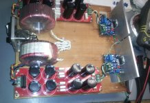
Attached is a power supply in use with 200va transformers for TDA7294 Monobloc amplifiers (each chip has its own transformer and power board).
Attachments
Following me? Nope. You didn't.
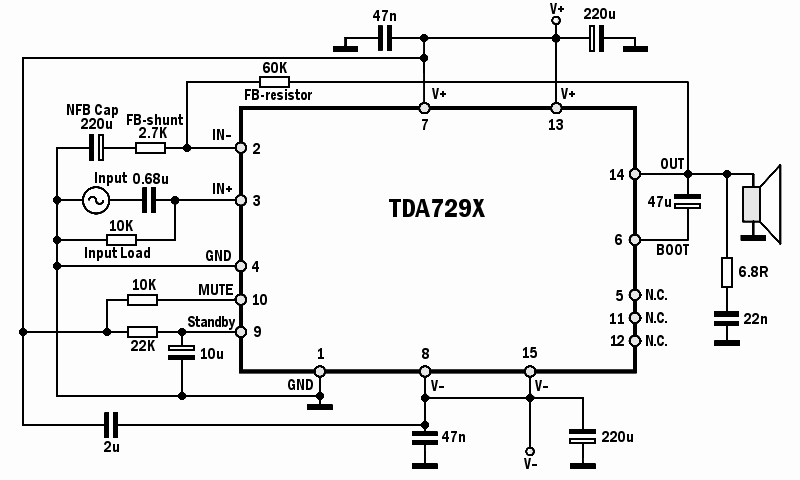
TDA7294 non-inverting amp:
Pair 220u amplifier board power caps and a single 2u polyester rail to rail.
47u (or 68u) for bootstrap
10k for input load resistor
10k for mute (no cap)
22k with 10u timer for standby
60k (120k||120k) for feedback resistor
2.7k for feedback-shunt resistor
220u (or more) for NFB cap
1u (or less!) for input
Output zobel is 10n with ~8R
Add RF filtering to input cap
Use a stiff power supply (20,000u per rail, 3a per chip)
Use less voltage than max (under-volt)
Oops... I thought you meant 2x220uf per rail. As I have space for one pair on pcb so I took 470uF. Will try 2x220...
TDA7294 is not a gainclone. The bigger the amplifier board Power circuit capacitance, the duller TDA7294 will go (similar to some discrete amplifiers). I think we should use only as much as necessary to prevent shout.
To my ears, with 470uF the amp already shouts. I can hear that the problem (distortion) is with female vocal (shouting).
Well, that's very strange. My own TDA7294 is very hard to tell apart from the LM1875 projects, or my PA amp, none of which are either depressing or fatiguing. An unoptimized TDA7294 should sound about as good as an STK
Well, this is the reason why I'm building your version (and I have built many versions). To prove to myself that I know exactly what I hear.
Trying to guess what could be the problem:
DC offset and/or fake chip cooked a tweeter? (needs speaker protection)
Bad quality NFB cap used? (try paralleling a tiny bypass cap)
Input cap was larger than 1u? (try 0.68u)
Bad/overlarge amplifier board power caps? (try replacement 220u)
Very dulling power supply? (try the diode trick)
Speaker negative sent to the power board? (try the amp board 0v)
Bias fail from under-volting? (try 35+35VDC power)
Printed circuit board layout issues? (replace or omit)
Accidental tone control installed somewhere? (debug)
No offset, very silent. Used 2 speakers. Main one is for testing amplifiers: a full-range driver (no crossover, no tweeter).
For FB cap I used Nippon Chemicon SM-D Bipolar 2x100uF. Will replace one with 47n-100n, whatever fits on the pcb.
Input cap was 1uF (fit well on PCB). Will try lower values. I think a WIMA MKP will fit.
On-board 470uF will be replaced. Maybe with Philips 220uF.
Very dulling power supply? I think the amp is not dull, rather, it tries to mimic other sweet sounding chip amps, which is not accurate imo (distortion with vocal). My power supply modules are for testing new amps. I have used 8x3300uF Nichicon, same value with your 12x2200uF. I used 2x4 hyperfast diodes. No bleeder.
Speaker ground is from PCB (as designed).
Yes, I agree underrated voltage (20V) is a problem. I think optimum is around 31V, as datasheet example to measure performance. Will use 28V as some on-board capacitors are rated 35V only (to fit on small pcb).
PCB is already good (have been used for many good sounding TDA7294 before). And I made it better with PTP and using solid copper wire along the high current track.
Experiment: Perhaps the lack of gain causes the source to strain (source not useful in that condition), so try feedback resistor at 100K to max out the gain and put the input load to 56K--slightly worse for the amp, but possibly help the source a lot.
Hmmm... I'm against such approach. What I'm doing here is trying to listen to TDA7294 setup that others are listening, so I can understand their comments about the sound. And BTW, I have always had benchmark amps next to the amp I'm playing with 😉
Oops... I thought you meant 2x220uf per rail. As I have space for one pair on pcb so I took 470uF. Will try 2x220...
So I tried 2x220uF. I couldn't find my Black Gate. My options were Philips, Cerrafine, Panasonic Pureism (which I don't like) and Panasonic CE HF. The Panasonic is twice the size of Cerrafine (and I think only slightly smaller than BG) so I used that.
I'm afraid I was listening to different brand instead of different capacitance here 😛 But I also change the bootstrap cap from 2x33uF Elna to Philips KO (that I like) 68uF.
Didn't want to change too many things at once. But alas, I changed the location of the main speaker 😡
The first moment I heard the sound, I didn't recognize the sound of TDA7294 I have been familiar with. With the last change the sound is less gorgeous but more musical. I like the latest setup with 2x220uF, whatever causing it 😀
But still, ehm, it's a chip amp 😱
I don't know why, I feel disturbed with the sound of this amp... But not by my other TDA7294 amps... Even with the same power supply...
Jay, You are miles ahead of me ( I'm still working on some graphics to keep things defined for we less experienced) but I did find some 220 U caps to try. Unfortunately, they are all large amd previously used. Is simple off-board mounting OK, or should I attempt to extend the leads ? (I've done that before successfully)
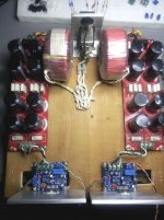
I'm working on the dual transformer setup right now.
I'm working on the dual transformer setup right now.
Attachments

Unfortunately, they are all large and previously used. Is simple off-board mounting OK, or should I attempt to extend the leads ? (I've done that before successfully)
I'm working on the dual transformer setup right now.
Caps have very long useful life (when not abused of course). What Daniel has done here is "tweaking". As he said, every pcb trace has its own parasitic inductance. You need to "tweak" it to find the sweet spot. With 220uF I think I don't want to have more than 4 cm (no technical justification here) from IC pin, and that is with solid wire/trace. Bypass cap is a must (100n direct on pin).
Contrary to "tweakers", more technically minded people will usually prefer technical approach to solve problems. I myself think that both must be employed, where tweaking should be done at the end after more technical approach has been employed. And I also always think about price to performance ratio. What I mean here is, I don't like to invest too much money for quality parts just to get a cheap sound. Discrete amps clearly more enjoyable for me.
If I try to find an optimum output for TDA7294, I will first find the issues to be solved. And I will pick two: power supply noise and input impedance. Work it out and finally tweak it by ears. I will start (actually I have) from here: ÓÌÇ× ÍÀ ÌÈÊÐÎÑÕÅÌÅ TDA7294
Attachments

amplifier board power caps
Bob those 50v 220u with the "M" are Panasonic, and may do nicely.
The amplifier power caps need to be quite close to the amplifier chip.
Those are about normal size for the amplifier board's power caps.
Maybe see if there's room to add a small drilling to the board (so that normal size caps can fit) without drilling through a trace?

A few notes on the TDA7294...
The schematics of the 'insides' are notional only and not the actual schematic. Someone mentioned an op-amp as a phase inverter for the bottom MOSFET, in actuality this is a rather different circuit.
The output stage uses a combination of current source and bootstrap to enable the 'VAS' stage to produce outputs above the positive rail in order to be able to fully switch on the top MOSFET in the output stage. In some cases omitting this mechanism actually produces better sonical results even though there is a reduction in power. The reason is capacitive coupling of the bootstrap circuit to the VAS recycling any crossover distortion into nonlinear current sourcing for the VAS. It is a subtle difference, and can be avouded by driving the input stage power supply to about 8V above the output stage power supply.
In cases where separate power is provided to the input stage, it is VITAL there is a schottky diode preventing the input stage negative power rail ever going more more positive than the output stage negative power rail. The reason for this is the negative input stage power rail is tied to the chip's substrate (and with it the cooling tab), this should always be the most negative part of the chip otherwise parasitic thyristor structures which normally provide insulation of circuit parts from the substrate latch into conduction turning the chip into a short circuit, resulting in catastrophic failure when full power is applied (chips will literally blow apart). This is only hinted at in the datasheet in the 'high efficiency application circuit' - actually a class G amplifier built around the chip.
The most improvement in distortion comes from providing a regulated more negative rail for the input stage, as the first stage of the chip amp has lower PSRR from the negative rail. Adding a regulated and more positive supply rail for the input stage is mainly useful to eliminate the bootsrtap cap for the output stage - a higher input stage positive rail will automatically provide the extra voltage needed to drive the top MOSFET in the output stage to full conduction.
It is highly advisable to use the chip derated, in a configuration with lower than maximum output power. 30-40W has proven to be completely reliable and optimizeable without ever reaching any of the chip's maximum ratings. In particular, the power dissipation rating is a problem, the case will not dissipate as much heat as the actual silicon might suggest from it's voltage and current ratings. Think of these as a 'reserve'. The chip will reward you with top performance as none of it's protection circuits will ever be activated and muddle up the music signal.
The input stage is fairly low noise, but it's still preferable to keep input and feedback impedances low, better 10 or 20k than 50 or 100k. Keeping the DC resistance on both the + and - input is crucial for low offset, also if somewhat lower amplification factors are used (IIRC 20 or 24 is the minimum for stable operation), I have found the chip's input stage offset to be low enough for the feedback DC nlock capacitor to be eliminated entirely.
Input stage decoupling does not have to be excessive and the chip works with fairly long supply lines to the input stage quite well. On the other hand, keeping all the output stage loops as short as possible is HIGHLY desirable. Output stage decoupling is very important and more so with respect to low ESR than actual capacitance values. Also keep the output boucherot RC cell grounded as close as possible to the star ground point of the local decouplers for the output stage.
DO NOT operate the chip without a heatsink, because the MOSFET output stage standing current is quite high and will cause the thermal protection to activate in a few minutes, producing utterly atrocious performance even at very low output levels 🙂
If a separate output protection circuit is used, so that the chip does not have to be put into standby or mute, an external current sink can be used to drive the output stage into partial single ended operation, i.e. a higher standing current / asymetrical crossover point amplifier, or even a full single ended class A amplifier up to some 10W or so. This is a power-OPamp 'translation' of the same technique used to drive regular OPamps into class A operation. By providing an external sink, the bottom MOSFET in the power stage is completely switched off and the phase splitter is inactive, making the top MOSFET operate in pure follower fashion. As long as the complete amplifier is asked to sink only as much current as the current sink provides, and the chip to source up to twice the current of the current sink, the output will remain symetrical and work purely in class A. 3 things to take care of here - firstly. the maximum current sourced from the chip is lowered by the current of the current sink WRT chip maximum rating, i.e. maximum current at which the overcurrent protection in the chip will engage. Secondly, observe the maximum dissipation limit, this is a point where the chip is somewhat deficcient so an implementation like this will have to be seriously derated WRT output power as the current sink's current increases. Thirdly, keep in mind that the chip's standby/mute circuitry does indeed put the chip into standby and switches off it's output, but has no idea there is an external current sink - if the chip is put into standby with the current sink turned on, the sink will gladly pull current through your speaker into the negative power supply, potentially destroying your speakers. In theory one could also control the sink with the standby signal, however because it's virtually impossible to make both come on and off completely in sync, there will be a transient as it turns on and off. The proper complex way to do this would be to turn on the chip, turn on the sink (preferably a soft start function should be built into the sink), then unmute the chip. Reverse operation for switching it off, keeping in mind a power supply dropout might not give you enough time to do a soft stop on the sink!
Although it is possible to use a current source instead, this is not optimal. Instead of the bottom MOSFET in the output stage being turned off, it will turn off the top MOSFET which requires the bottom half including the phase splitter to do all the work, requiring the signal to go through the additional circuitry of the splitter, and also because the bottom half works in common source mode, requiring the NFB loop to do more with a 'longer' and thus more phase shift prone circuit. Unlike this, the top part is a straight follower from the VAS, the quickest and shortest way out the power stage.

That's a bunch of information. Will require several readings to absorb. What I believe I'm hearing is, along with gootee's posts, full optimization will require a more sophisticated board layout than what is generally used. Is that correct and are you aware of any attempts to design that animal?
I finished the dual transformer setup, but won't do any serious listening till tomorrow morning.
I finished the dual transformer setup, but won't do any serious listening till tomorrow morning.
Attachments
Last edited:
That takes the idea of tweaking to a whole, new level. 🙂 While that may be viewed as a challenge for some, I wonder if the sonic characteristics improvements - in terms of 'real' significant differences - offset a total re-design of the amp? That sounds like a real commitment of time, money and a lot of energy. Just a thought. I'm quietly and passively following this thread though.....full optimization will require a more sophisticated board layout than what is generally used.....
redjr, I understand what you are saying. It does appear two divergent paths are emerging. I'm coming here from a LM3886/MyRef background and completely appreciate the years and number of contributors necessary to go from "ChipAmp" to it's current state. Maybe this thread will determine which direction gains the most support.
A few notes on the TDA7294...
The most improvement in distortion comes from providing a regulated more negative rail for the input stage, as the first stage of the chip amp has lower PSRR from the negative rail. Adding a regulated and more positive supply rail for the input stage is mainly useful to eliminate the bootsrtap cap for the output stage.
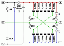
Thanks for the info, ilimzn. I'm attaching your circuit to this thread so everyone can see it as an option to optimize the TDA7294 output (by regulating the input stage).
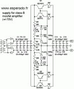
I myself prefer another option to retain the bootstrap cap. And regulation can be done to entire amplifier. Call it a pre-regulation, because full regulation for output stage of class-B amps usually doesn't sound good for some of us. So a simple zener based pre-regulator can be employed. I'm attaching a power supply used by esperado (Christophe) to power his mosfet amplifier (class-B SAA-Crescendo). Note that after regulation he still provides massive capacitance. I have tried simpler than this and I can accept the sound, noting that I'm a proponent of input-stage-only regulation.
The regulator must be simple, as too expensive might not justify the use of chip amp (?). Fortunately we don't want a full regulation for the output stage. What is your comment about this second option?
As for going "cost-no-object" with this cheap chip amp, can you see any benefit? As you have noticed, it is not really preferable to get the maximum power out of it. About class-A approach, I'm afraid an Aleph-J is simpler and sound better. What I can see is the performance of the mosfet. They say it is a DMOS. But I think it s quite good for class-B. So because lateral mosfets are expensive, this can be a justification for those who like the sound of mosfet amps.
Attachments

Last edited:
The input stage is fairly low noise, but it's still preferable to keep input and feedback impedances low, better 10 or 20k than 50 or 100k. Keeping the DC resistance on both the + and - input is crucial for low offset, also if somewhat lower amplification factors are used (IIRC 20 or 24 is the minimum for stable operation), I have found the chip's input stage offset to be low
Yes, I can see the current mirror of the input LTP. With original schematic I prefer lower feedback resistance (10K for example). But low input impedance (issue for the signal source), along with low feedback (issue for speaker damping) will seriously "ruin" a capacitive mosfet output performance. You will see lower distortion, but the sound will be boring. And this is a situation I think where a matching preamp should be discussed also, as part of the design.
But the schematic from radiolub that I posted previously have a high input impedance and to my ears sound preferable than any schematics with simple FB arrangement I have tried.
Power dissipation is not always a problem since latfet/dmos/powermos is very efficient. I actually use mine at up to 127 watts with 4 ohm speakers and it requires only a 3"x3"x2" heatsink that doesn't even run hot. It is power circuit options that provide the cool. And, that cool came along with clear sound, directly proportional and related. Yes, a hot running TDA7294 is atrocious, so the easy answer is don't run it hot. 🙂 Mine is simple bus rail, except. . .It is highly advisable to use the chip derated, in a configuration with lower than maximum output power. 30-40W has proven to be completely reliable and optimize-able without ever reaching any of the chip's maximum ratings. In particular, the power dissipation rating is a problem, the case will not dissipate as much heat as the actual silicon might suggest from it's voltage and current ratings. Think of these as a 'reserve'. The chip will reward you with top performance as none of it's protection circuits will ever be activated and muddle up the music signal.
. . . the MOSFET output stage standing current is quite high and will cause the thermal protection to activate in a few minutes, producing utterly atrocious performance even at very low output levels 🙂
This is not 127 real watts as there is an couple of exceptions that work dynamically. I have employed a peak filter from the hardware store in order to slam something other than the output devices. This is 3 conductors of 20ga solid copper thermostat wire (in the range 5" to 8"), twisted and used as the umbilical cable in-between the power board and amplifier board. . . and then the discharge of the 220u amplifier board power caps is not enough to hammer the outputs. I'll talk about that in the next post because bigger power handling capacity was merely accidental, and not the primary reason for doing it.
- Home
- Amplifiers
- Chip Amps
- Optimizing TDA7294 Output