After listening tests of my pre standard II JFET preamplifer, and upon requests of the builders, I have decided to design a new version of the Dipre 2 preamplifier, Dispre 2 - JFET.
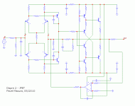
The main difference is that Dispre 2 – JFET has Toshiba 2SK170/2SJ74 devices in the input stage, not the bipolar transistors that were used in the Dispre 2 V4. This modification resulted in a design of a new PCB board, as it was impossible to simply replace BJTs by JFETs, circuit modification of the input stage had to be made. At the same time, I added two resistors to enable setting of the output stage idle current. These resistors allow, in case of high technology spread of output devices, to tune output stage idle current.
Dispre 2 – JFET can be also used as a headphone amplifier, without any components changes needed.
Dispre 2 – JFET has complementary differential circuit topology with self biased JFET input stage (this topology was introduced by John Curl). This maximizes linearity of the input stage and distortion suppression does not rely only on an overall negative feedback. To remove output DC voltage component, DC servo is used.
Output stage idle current is set at 40mA, and it works in a class A up to 8V into 100 ohm load. For standard link load 600 ohm and higher, the output stage works in a class A for the whole range of output voltage up to clipping.
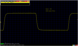
Dispre2 - JFET has wide bandwidth and high slew rate again, similarly as Dispre 2 V4.
Regarding PCBs, please visit a thread here:
http://www.diyaudio.com/forums/vendors-bazaar/166049-dispre-ii-pcbs-available.html
or check my webpage: Dispre 2 -
The main difference is that Dispre 2 – JFET has Toshiba 2SK170/2SJ74 devices in the input stage, not the bipolar transistors that were used in the Dispre 2 V4. This modification resulted in a design of a new PCB board, as it was impossible to simply replace BJTs by JFETs, circuit modification of the input stage had to be made. At the same time, I added two resistors to enable setting of the output stage idle current. These resistors allow, in case of high technology spread of output devices, to tune output stage idle current.
Dispre 2 – JFET can be also used as a headphone amplifier, without any components changes needed.
Dispre 2 – JFET has complementary differential circuit topology with self biased JFET input stage (this topology was introduced by John Curl). This maximizes linearity of the input stage and distortion suppression does not rely only on an overall negative feedback. To remove output DC voltage component, DC servo is used.
Output stage idle current is set at 40mA, and it works in a class A up to 8V into 100 ohm load. For standard link load 600 ohm and higher, the output stage works in a class A for the whole range of output voltage up to clipping.
Dispre2 - JFET has wide bandwidth and high slew rate again, similarly as Dispre 2 V4.
Regarding PCBs, please visit a thread here:
http://www.diyaudio.com/forums/vendors-bazaar/166049-dispre-ii-pcbs-available.html
or check my webpage: Dispre 2 -
Attachments
Hi Bogdan, this is a good question. I will try to review older results and return with them later. According to my previous experience, it was more an issue with bipolar than with JFET input stage.
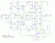
Now I am attaching a schematic with part numbers, to simplify possible discussion.
Now I am attaching a schematic with part numbers, to simplify possible discussion.
Attachments
I would aim for 0.5% to 1% of half the rail to rail voltage supply.
+-15V PSU and servo correction for <=+-150mV.
If it exceeds the servo correction range then a DC detect and mute should trigger on the output.
Andrew, do you speak about input or output DC. In case it was output DC, I would suggest wider correction range.
Regards,
I am thinking input range error correction. With a 4times gain stage that would give an output correction range of +-300mV to +-600mV.
But I do want to hear your opinion/design parameters.
Thank you for the clarification. For the former version, Dispre 2 V4 BJT, I was correcting up to 600mV of the input DC offset voltage. For this JFET version I expect to correct less DC voltage.
Regards,
I have question ?
Is there any correlation between high input capacitance of the circuit and little bit boring (laid back) sound reproduction ?
Q. came to my mind after listning expirience with Borbely simple pre
( folded cascode , jfet input compl diff+ jfet VAS + jfet output buffer A-clas 10mA )
Is there any correlation between high input capacitance of the circuit and little bit boring (laid back) sound reproduction ?
Q. came to my mind after listning expirience with Borbely simple pre
( folded cascode , jfet input compl diff+ jfet VAS + jfet output buffer A-clas 10mA )
I am using a somewhat similar topology in my High Z MPP phonostage and first it did sound less dynamic then the BJT variety. After playing around with iddle current and circuit values i got it working to my full satisfaction. Nowerdays i am using Fets at the input of most of my stages.
Excuse me PMA for I am no expert... but I would like to ask... output from Q5 and Q6 has no 'real' load? My studies suggest that this output is current and best into a pre-defined load, such as a resistor to ground (in parallel with the input of the output stage) ? i.e. a resistor from collectors of Q5, Q6 to ground?
J.
J.
Now I am attaching a schematic with part numbers, to simplify possible discussion.
What range of values for R7 and R12?

I am using a somewhat similar topology in my High Z MPP phonostage and first it did sound less dynamic then the BJT variety. After playing around with iddle current and circuit values i got it working to my full satisfaction. Nowerdays i am using Fets at the input of most of my stages.
Hi Joachim, yes some play with resistor values is needed to get both most linear LF operation and minimalization of non-linear capacitance effect.
Regards,
Excuse me PMA for I am no expert... but I would like to ask... output from Q5 and Q6 has no 'real' load? My studies suggest that this output is current and best into a pre-defined load, such as a resistor to ground (in parallel with the input of the output stage) ? i.e. a resistor from collectors of Q5, Q6 to ground?
J.
Hi Jen, I played with that in the previous version, and finished with no resistive load of the VAS.
Regards,
What range of values for R7 and R12?
Dear Nelson, they are to be estimated during evaluation tests.
Regards,
in other words ask for additional cascode in the jfet input compl diff circuit ( as an option), will not meet our positive feedback
I tried both, for the preamp with 2 x 15V supply I do not assume to use the cascode.
Regards,
Nelson is obviously most expirienced around here so maybe he want to answer my question,when designing a preamp what you consider the worst case input dc-voltage (offset) that servo must remove? I`m thinking about the dc offset voltage that comes from the source to the preamps input.
Cheers Borko.
Cheers Borko.
- Home
- Source & Line
- Analog Line Level
- Preamplifier Dispre 2 - JFET