John, Good to hear your doing better, and you have more time for enjoying some of the better parts of life, DIYAudio! We are all pulling/or pushing for you, get well buddy...😀 😀 😀
Lee
Lee
This may be really dumb, but here goes:
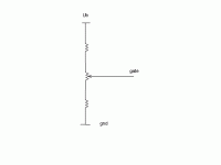
Why couldn't a bifilar wound choke have one end of its inputs connected to the drain and source pins of a transistor and the other ends to the speaker? This arrangement would require dc blocking caps... and an air wound choke has resistance...
or: 1/2 the bifilar choke could be the source pin resistance and the the other half, the drain pin resistance. Hummm... the idea is to get the chokes to cancel out the magnetic saturation qualities (granted, an air choke doesn't saturate). Then we couple the speaker to the drain and source pins.
It just struck me, so out it came,
sorry in advance if this is stupid,
John🙂
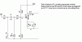
regarding the drawing above:
I've just begun to read Mr. Borbely's papers on jfets and noticed that he has an arrangement very similar to my cut and paste drawing of Nelson's artwork. He differs in that he uses source resisters beneath each jfet, rather than beneath the current source.
Gosh, this stuff is fascinating!
John🙂
I've just begun to read Mr. Borbely's papers on jfets and noticed that he has an arrangement very similar to my cut and paste drawing of Nelson's artwork. He differs in that he uses source resisters beneath each jfet, rather than beneath the current source.
Gosh, this stuff is fascinating!
John🙂
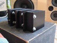

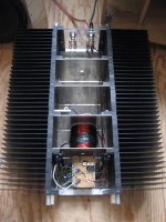


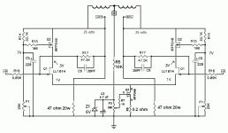
I finally finished my amp and power supply. I've got her almost dialed in. There is a bit of a problem with the bias adjustment: it's twitchy and won't stay anywhere near 50mv dc offset.
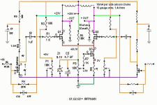
I ran R3 to the positive rail, now I'm wondering if it's necessary to have it returned to its original location (local feedback).
All suggestions welcome.
John🙂
I ran R3 to the positive rail, now I'm wondering if it's necessary to have it returned to its original location (local feedback).
All suggestions welcome.
John🙂
Attachments
carpenter said:I finally finished my amp and power supply. I've got her almost dialed in. There is a bit of a problem with the bias adjustment: it's twitchy and won't stay anywhere near 50mv dc offset.
I ran R3 to the positive rail, now I'm wondering if it's necessary to have it returned to its original location (local feedback).
All suggestions welcome.
John🙂
my brain is on red ...it's 0420 now at my place
try like this:
Attachments
Thanks Choky,
Beings that I'm an amateur, I'm not fully appreciating the difference between your circuit and Nelson's.
Possible errors:
I changed the location of R1 and R3. R1 used to be located on the outside of the biasing voltage divider; I moved it closer to the gain FET in order to keep it in close physical proximity on the pcb. R3 was originally tracking the drain voltage of the gain FETs and now it see only the positive rail. I'm wondering if it should once more be seeing the drain...
I'll be studying Nelson's other works with great interests tonight; perhaps there, I'll discover the answer.
I really appreciate your efforts and look forward to further enlightenment from you and this forum.
John🙂
Attachments
John
You are giving dc feedback to ZVP3310 gate, on purpose . . . ?
I would consider only ac signal feedback, blocking dc with caps.
Regards
You are giving dc feedback to ZVP3310 gate, on purpose . . . ?
I would consider only ac signal feedback, blocking dc with caps.
Regards
- Status
- Not open for further replies.
- Home
- Amplifiers
- Pass Labs
- ZV7-T (transformer)