Susan-Parker said:Hi,
Thanks. Please let us know how you get on.
Understood. And Agreed. This is hobby and DIY and meant to be relaxing etc. with personal enjoyment, satisfaction and learning.
I would probably look at using a standard MOSFET to give a reasonably regulated 11.75 volt supply as the extra couple of volts will make a big difference to the output watts possible.
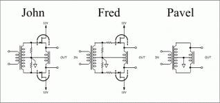
Note from my VMOS schematic that the gate zeners are reversed in polarity. And here should probably be reduced to 9 volts.
Also don't forget the current capability of the transformer windings, as with these high biases there will be some heating.
One of the problems seems to me to be the package as it isn't overly big for the types of currents and wattages proposed.
I know that it is theoretically capable of 65 watts but once one has derated at higher temperatures e.g 80 degrees C it is only about 30 watts and the package has a thermal resistance junction to case of 1.8 degrees/watt - compared to 0.69 for TO247
But high bias with low voltage is certainly one way to go.
Per STW34NB20 I use 750mA at 34 volts supply in my standard power stage.
Will be interested to hear how this version fairs.
Best wishes,
Susan.
Thanks for the notes Susan. I think this one is worth a shot. Actually, the hardest part seems to be getting the OPT's made, as they are not so typical. I may have to do them myself (referring to the wire ratings you had sent me via e-mail).
The mosfet regulated supply seems a good idea and should be pretty easy. Could try it with the unmatched STW FET's.
Zener issues noted.
Yeah, that package is small, but I think I can work something out there to remove heat. I'd have to shed about 10-12 watts per FET. My intended load conditions wouldn't add significantly to that.
This sounds like fun. Jkeny, you still in. How many?
Sheldon
edit: Susan, I would plan to use the split bobbin arrangement, as it seems easiest to get the the exact turns on each side. The larger wire means a bigger core but how about winding the secondaries with smaller wire, as they don't have to carry the current? It wouldn't be quite as neat, but maybe carefully wound quad filar, coupling would still be good.
Hi Sheldon,
Yes, you could do that, or even only tri-filar wind.
I use dual chamber quad filar of the same wire gauge to give me the most flexibility. Also for full range the low bass driver benefits (a bit) from having lowest DC resistance particularly for ported speakers.
However for your specific application tri should be fine.
Best wishes,
Susan.
Sheldon said:edit: Susan, I would plan to use the split bobbin arrangement, as it seems easiest to get the the exact turns on each side. The larger wire means a bigger core but how about winding the secondaries with smaller wire, as they don't have to carry the current? It wouldn't be quite as neat, but maybe carefully wound quad filar, coupling would still be good.
Yes, you could do that, or even only tri-filar wind.
I use dual chamber quad filar of the same wire gauge to give me the most flexibility. Also for full range the low bass driver benefits (a bit) from having lowest DC resistance particularly for ported speakers.
However for your specific application tri should be fine.
Best wishes,
Susan.
Susan-Parker said:Hi Sheldon,
Yes, you could do that, or even only tri-filar wind.
I use dual chamber quad filar of the same wire gauge to give me the most flexibility. Also for full range the low bass driver benefits (a bit) from having lowest DC resistance particularly for ported speakers.
However for your specific application tri should be fine.
Best wishes,
Susan.
Ah, yes. Tri filar would be the easiest for a 2:1 transformer.
Thanks,
Sheldon
Question on using the FET's: I was planning on using a resistor on each FET source. But what are the pros and cons of a common source resistor on the center tap of the transformer primary? This second method would seem most like the original design, which uses single bias source for both output devices. Using separate bias resistors would seem to make it easier to get balanced output, even if the FET matching is not perfect.
Sheldon
Sheldon
Hi,
The use of seperate bias ristors will still be tricky as the variations between to make an adjustment will be very small. Sub ohms at an Amp plus!
WIth a single shared resistor there is a virtual ground, which is prefered.
This resistor can be a nice robust wire wound type as it is not moving as part of the AC waveform, and so any inductance doesn't matter.
My VMOS line driver circuit stabilises at 300mA (approx) for the pair between 12 and 24 volts supply variation. (It does go up a little bit as the volts rise, but only a slight change on the meter needle.) This is optimum.
I am going to revisit the 6C33C tube PP version with the new Sowter input transformer and a virtual ground as per the VMOS circuit. Will post the the results when I do.
At the end of the day go with what you are comfortable with, and given the simplicty of the circuit trying both ways isn't overly onerious.
Best wishes,
Susan.
Sheldon said:Question on using the FET's: I was planning on using a resistor on each FET source. But what are the pros and cons of a common source resistor on the center tap of the transformer primary? This second method would seem most like the original design, which uses single bias source for both output devices. Using separate bias resistors would seem to make it easier to get balanced output, even if the FET matching is not perfect.
Sheldon
The use of seperate bias ristors will still be tricky as the variations between to make an adjustment will be very small. Sub ohms at an Amp plus!
WIth a single shared resistor there is a virtual ground, which is prefered.
This resistor can be a nice robust wire wound type as it is not moving as part of the AC waveform, and so any inductance doesn't matter.
My VMOS line driver circuit stabilises at 300mA (approx) for the pair between 12 and 24 volts supply variation. (It does go up a little bit as the volts rise, but only a slight change on the meter needle.) This is optimum.
I am going to revisit the 6C33C tube PP version with the new Sowter input transformer and a virtual ground as per the VMOS circuit. Will post the the results when I do.
At the end of the day go with what you are comfortable with, and given the simplicty of the circuit trying both ways isn't overly onerious.
Best wishes,
Susan.
Susan-Parker said:Hi,
The use of seperate bias ristors will still be tricky as the variations between to make an adjustment will be very small. Sub ohms at an Amp plus!
WIth a single shared resistor there is a virtual ground, which is prefered.
This resistor can be a nice robust wire wound type as it is not moving as part of the AC waveform, and so any inductance doesn't matter.
My VMOS line driver circuit stabilises at 300mA (approx) for the pair between 12 and 24 volts supply variation. (It does go up a little bit as the volts rise, but only a slight change on the meter needle.) This is optimum.
I am going to revisit the 6C33C tube PP version with the new Sowter input transformer and a virtual ground as per the VMOS circuit. Will post the the results when I do.
At the end of the day go with what you are comfortable with, and given the simplicty of the circuit trying both ways isn't overly onerious.
Best wishes,
Susan.
Thanks,
Yes, adjusting with small value resistors would be tricky. If I try that, I'll get precision resistors and adjust one or the other side a bit by adding a large value in parallel. Or make low value resistors by paralleling a bunch of higher value ones.
But I may just make the OPT's with a gap as you had mentioned via e-mail. That way, a small imbalance wouldn't be a problem and it would be fine for my application too, as I don't need the lower registers. By the way, I assume that a gap is made by stacking the E and I completely separately, then assembling with a thin shim (copper as you suggested) between the E and I?
Sheldon
Hi,
Yes, I do the following:
1. Assemble the E section to be a full stack in the wound bobbin (tightly fitted and squared up).
2. Place the two end shrounds either side and losely bolt them up through the E's holes. Tighten until the laminations start to "spring" (once you are doing this you will know what this is).
3. Using copper strip (with adhedsive, as used for EMC) I cover the entire width of the legs and center with one length of copper foil of a suitable thickness.
4. Place the I pieces (ensuring I have the same number as the Es).
5. Fit two remaining bolts and tighten up as per "2".
6. Check that the number of Es and Is match!
7. Walk the bolts tightening them up in a couple of rounds.
Hope this helps.
Best wishes,
Susan.
Originally posted by Sheldon
But I may just make the OPT's with a gap as you had mentioned via e-mail. That way, a small imbalance wouldn't be a problem and it would be fine for my application too, as I don't need the lower registers. By the way, I assume that a gap is made by stacking the E and I completely separately, then assembling with a thin shim (copper as you suggested) between the E and I?
Yes, I do the following:
1. Assemble the E section to be a full stack in the wound bobbin (tightly fitted and squared up).
2. Place the two end shrounds either side and losely bolt them up through the E's holes. Tighten until the laminations start to "spring" (once you are doing this you will know what this is).
3. Using copper strip (with adhedsive, as used for EMC) I cover the entire width of the legs and center with one length of copper foil of a suitable thickness.
4. Place the I pieces (ensuring I have the same number as the Es).
5. Fit two remaining bolts and tighten up as per "2".
6. Check that the number of Es and Is match!
7. Walk the bolts tightening them up in a couple of rounds.
Hope this helps.
Best wishes,
Susan.
Susan-Parker said:Hi,
Hope this helps.
Best wishes,
Susan.
It does, thanks. I'll have a better idea once I actually wind the bobbin and put stuff together.
Sheldon
jkeny said:suiraMB,
This sounds excellent - but I'm not a tubes guy - any chance of your take on a schematic?
Just use Susan's regular schematic, but make sure the primary windings of the transformers have enough DC resistance.
Essentially, pick your suppy voltage, then pick an idle current that will keep the device dissipation down to about 10W each. Find the Vgs value that will give you the right current at your supply voltage, and make the transformer so that the primary winding DC resistance multiplied by the idle current gives you that Vgs drop.
In order to cool them properly, I'd recommend the suggestion form someone in another thread, namely putting indium solder on a heatsink, then heating that until the indium solder melts, then using a vice to press the devices against the heatsink until the indium solder cools again. This will give very good heat transfer characteristics.
I will try to order some jFets- although Europe group buy is finished through Steen.
You'll need to find someone who can send them to you from the US, since it's too much hassle for Mr. Rollins to ship them to Europe due to postal service and bank problems.
Or you could buy 2000 units from Lovoltech 😱
I will use toroid mains transformers to test - will these satisfy the high primary DC condition you mentioned?
I doubt it. But if you're just testing, you can put a resistor in series with the source pins to get additional resistance.
Sheldon said:If I looked at the correct device, it appears that they are rated to 25V. This would only allow a max. 12V rail, as the FET sees twice the rail voltage, due to the neg. voltage developed by the transformer.
Correct, they can only handle 25V, limiting the rails to 12V. But you can use a step-up output transformer.
With 7mOhm source impedance and the possibility of paralelling several devices (a necessity for high output power, unless you use a fan on the heatsink, as well as the indium-solder trick, in which case I guess you could probably reach 20W dissipation per device), you can use a fairly large step-up ratio.
Note that, while the voltage is limited, the devices can quite easily deal with 100A peaks if their total dissipation is kept within sane limits.
If you need significantly higher dissipation, and have a lot of cash to burn (or a lot of people in a group buy), you could order the devices in chip carrier form (~€2000 minimum), along with some 1200V SIT power JFETs from SemiSouth (~€1000 minimum). SemeLab UK can then package these in a high-dissipation package. This gives you pretty much any voltage rating you might care to use, along with a massive power handling.
Of course, the SemiSouth devices by themselves could probably do the trick. Being silicon-carbide devices, they can operate at whatever temperature the leads can handle (well, up to about 800 deg C
 ).
).Sheldon said:In my previous post, I referenced a discussion about variation of Crss with output and its possible effect on phase related distortion. It looks like these FET's go from about 300pf at 20Vds to 600pf at 0Vds.
Correct, JFETs have a more favourable capacitance characteristic. If you want even better high frequency performance, you could try to drive them with an LSK170C buffer at 15mA bias or so.
I believe John Curl also suggested simply adding a polystyrene capacitor to swamp the nonlinear input capacitance to reduce distortion. In this case, 6nF should be enough.
So I could step than down 4:1 for a 25V swing and a Zout of 500, which would give a corner frequency of 500kHz.
You will want to make sure your arrangement does not exceed the Vgs limits (12V, I believe). Not sure this is a real problem, though.
If you are right about the distortion suiraMB, it should be no problem even going 1:1.
Actually, I think you could go 1:2 or even 1:3 without a problem. These devices handle a lot more current than voltage.
I have little concern about the output impedence as I will be using these for driving only frequencies higher than about 300Hz.
Don't make that mistake. Maintain a damping factor of about 25 or so at the driver's resonance frequency. Even midranges need some electrical damping to behave properly.
But, the bias power would have to be dissipated by the transformer. Wouldn't it be easier just to add some series resistance and get rid of the heat there?
That would indeed probably be simpler, but the DC resistance requirement to bias the JFET is not all that difficult to reach.
For example, at 4V 5A, you only need to drop about 1V. Of course, you'll be wanting 12V and 1A or so per device with your battery design, so you'll need to drop somewhat more.
Susan,
The depletion MOS devices are indeed interesting. I've been considering them to drive my Stax earspeakers.
However, power JFETs apparently have significant sonic benefits. Also, the higher current handling gives better control of difficult loads.
Of course, as many have pointed out, the low voltage handling means you either need a step-up OPT or a cascode if you want higher power handling.
However, their dissipation handling (especially with the indium solder trick and a big heatsink or a fan) should allow for enough power to drive modestly efficient loudspeakers (90dB+) to adequate listening levels. Since the circuit operates in class AB, you should be able to get 25W or so from a single pair with regular heatsinking, or 50W from a single pair with the modified heatsinking. This at high bias.
One approach which will let you bias the devices at high current, while dealing with high supply voltages, at the cost of some added complexity in the PSU is as follows:
Shunt regulated version:
Start off with a regular PSU (CLC, CRC or what-have-you), then feed the transistors through a series resistor that is capable of dropping a large voltage. Put in a P-channel mosfet with its source to the drain of the JFET(s), its gate to the source of the JFET(s) and its drain to the other rail, one for the "push" JFET(s) and one for the "pull" JFETs.
This acts as a shunt regulator, giving a Vds of 2-4V for the JFET. Assuming the P-ch MOS has a Vgs of 3V, you would need a transformer primary DC resistance of 0.2ohm to get 2.5A bias current.
Series regulated version:
Start off with a regular PSU. Follow up with a balanced series voltage regulator, using a 2SK389 or LSK389 (matched 2SK170 or LSK170 will do) Son-of-Zen-like differential stage, and followers on the outputs of the regulator.
Use a polystyrene or mica cap to superimpose the AC waveform on the reference voltage. Make sure the gain is around unity (varying it around unity can cancel some distortion, though, if you have an analyzer).
This approach will dissipate less than the shunt regulator on average, although it does interact more directly with the signal path. It does assure that you will be able to easily select an exact Vds value for the power JFET, though.
To protect the regulator, as well as the output, just add an I/V foldback (or SOA protection) to the regulator. It will not have the same sonic impact there as it would have in the output stage itself.
I could draw up a schematic to explain better, but I don't have any nice CAD software lying about, so it'd be a digital photograph of a sketch on paper.
Of course, both these approaches shift the bulk of the dissipation elsewhere. The series-pass regulator additionally reduces the net dissipation somewhat.
Of course, a properly filtered buck-converter tracking the signal could reduce the dissipation to an insignificant point, although the audio police (who have rarely seen a properly filtered converter, nor one combined with a linear regulator) would probably shoot anyone attempting this.
If you want more power, use the series regulator, make several primary windings (one per power JFET), put one JFET on each primary, and series-couple the secondaries for a very large step-up ratio. As noted, these things can be operated at Vds values from 0.1V and up, and their peak current would allow a fairly massive output if you idle them at lower power (something I understand to work well in this topology).
As noted, a source drop of about -1V at 3V drain-source gives you about 2.5A bias per device, for 7.5W average dissipation. With the mentioned heat sinking tricks, you then have 12.5W to spare, which means you can have very large dynamic peaks without overloading the output devices.
The Sony 2SK60 devices would of course perform better, given their higher dissipation ratings and voltage tolerances, but they are pretty expensive, being out of regular production.
In short, the Lovoltech devices should perform adequately by themselves if you don't need a lot of power, and if you do need a lot of power, you can use a step-up OPT and/or use a PSU regulator to achieve the equivalent of cascode operation, along with paralelling devices. And, unlike MOSFETs, the JFETs work fairly well at lower idle dissipation.
In any circuit, the semiconductor devices are generally the greatest obstacles to performance. Given that, I believe it will be worthwhile to make the extra effort to maximize their performance. And for those of us who can make do with 25W or so, it is no problem to get this from a single pair of devices without the added complexity I outlined.
Good stuff suiraMB
Cool idea. Any particular types to look for? I'd assume the lowest melt temp available. Good sources, if not available through Digikey, etc..
Wouldn't a step up output transformer raise the output impedence a bit high. I'm assuming something like 0.5-1R for biasing?
Another interesting idea. My driver has an impedence of abourt 3-4K. To get to about 22Vpp I have to step down about 9:1, which gives me abour 40-50 ohm reflected impedence. Should be able to drive a 10nf cap no problem.
suiraMB said:
In order to cool them properly, I'd recommend the suggestion form someone in another thread, namely putting indium solder on a heatsink, then heating that until the indium solder melts, then using a vice to press the devices against the heatsink until the indium solder cools again. This will give very good heat transfer characteristics.
Cool idea. Any particular types to look for? I'd assume the lowest melt temp available. Good sources, if not available through Digikey, etc..
suiraMB said:
Correct, they can only handle 25V, limiting the rails to 12V. But you can use a step-up output transformer.
With 7mOhm source impedance and the possibility of paralelling several devices (a necessity for high output power, unless you use a fan on the heatsink, as well as the indium-solder trick, in which case I guess you could probably reach 20W dissipation per device), you can use a fairly large step-up ratio.
Note that, while the voltage is limited, the devices can quite easily deal with 100A peaks if their total dissipation is kept within sane limits.
If you need significantly higher dissipation, and have a lot of cash to burn (or a lot of people in a group buy), you could order the devices in chip carrier form (~€2000 minimum), along with some 1200V SIT power JFETs from SemiSouth (~€1000 minimum). SemeLab UK can then package these in a high-dissipation package. This gives you pretty much any voltage rating you might care to use, along with a massive power handling.
Of course, the SemiSouth devices by themselves could probably do the trick. Being silicon-carbide devices, they can operate at whatever temperature the leads can handle (well, up to about 800 deg C
Wouldn't a step up output transformer raise the output impedence a bit high. I'm assuming something like 0.5-1R for biasing?
suiraMB said:
Correct, JFETs have a more favourable capacitance characteristic. If you want even better high frequency performance, you could try to drive them with an LSK170C buffer at 15mA bias or so.
I believe John Curl also suggested simply adding a polystyrene capacitor to swamp the nonlinear input capacitance to reduce distortion. In this case, 6nF should be enough.
Another interesting idea. My driver has an impedence of abourt 3-4K. To get to about 22Vpp I have to step down about 9:1, which gives me abour 40-50 ohm reflected impedence. Should be able to drive a 10nf cap no problem.
suiraMB said:
You will want to make sure your arrangement does not exceed the Vgs limits (12V, I believe). Not sure this is a real problem, though.
I'll add the protection diodes as shown in Susan's schematic (something less than 12V)
suiraMB said:
Maintain a damping factor of about 25 or so at the driver's resonance frequency. Even midranges need some electrical damping to behave properly.
I'd have a pretty high damping factor at a 2:1 stepdown ratio. Even 1:1 would be fine I think. Or am I intrepreting the bias resistance incorrectly for calculating impedence, as the follower acts more like a current source? I have to think about this one some more.
Sheldon
Sheldon said:Good stuff suiraMB
Thank you. 🙂
Cool idea. Any particular types to look for? I'd assume the lowest melt temp available. Good sources, if not available through Digikey, etc..
Actually, the maximum operating/storage temperature is 150 degrees Celsius, so anything that melts at less than 120 C or so should be fine. In fact, a higher melting point allows you to run the devices hotter without the solder melting 🙂
Wouldn't a step up output transformer raise the output impedence a bit high. I'm assuming something like 0.5-1R for biasing?
A step-up OPT raises the impedance of the secondary, yes, which is why you want to wind it for a low secondary resistance. The AC impedance (given a low DC resistance) is negligible, as the LU1014D has 7mOhm Rds(ON) and 20S transconductance. This gives a 57mOhm source impedance for the transformer primary, I think. Although it's 6am here now, so I could be wrong. 🙂
Another interesting idea. My driver has an impedence of abourt 3-4K. To get to about 22Vpp I have to step down about 9:1, which gives me abour 40-50 ohm reflected impedence. Should be able to drive a 10nf cap no problem.
Indeed. Although with modern signal sources you routinely get 2-3Vrms at low impedances, so you could just drop the driver stage and turn your 9:1 around. If your source is higher impedance, a 2SK389V or LSK389C buffer would probably distort less with the same drive capacity.
I'd have a pretty high damping factor at a 2:1 stepdown ratio. Even 1:1 would be fine I think. Or am I intrepreting the bias resistance incorrectly for calculating impedence, as the follower acts more like a current source?
The damping factor is based on the DC resistance of the secondary, and the reflected AC impedance. Primary DC resistance does not figure into it.
The reflected AC impedance is RdsON + 1/Gm, divided by the turns ratio, and for a 4 ohm driver you need a reflected impedance plus secondary DC resistance of 0.400 ohms or less to maintain a damping factor of 10 or better.
0.057 ohms reflected through a 1:4 step-up would be 0.228 ohms, leaving almost 0.2 ohms for the DC resistance of the secondary.
suiraMB said:Actually, the maximum operating/storage temperature is 150 degrees Celsius, so anything that melts at less than 120 C or so should be fine. In fact, a higher melting point allows you to run the devices hotter without the solder melting 🙂
I'll chase some up.
suiraMB said:
A step-up OPT raises the impedance of the secondary, yes, which is why you want to wind it for a low secondary resistance. The AC impedance (given a low DC resistance) is negligible, as the LU1014D has 7mOhm Rds(ON) and 20S transconductance. This gives a 57mOhm source impedance for the transformer primary, I think. Although it's 6am here now, so I could be wrong. 🙂
The damping factor is based on the DC resistance of the secondary, and the reflected AC impedance. Primary DC resistance does not figure into it.
The reflected AC impedance is RdsON + 1/Gm, divided by the turns ratio, and for a 4 ohm driver you need a reflected impedance plus secondary DC resistance of 0.400 ohms or less to maintain a damping factor of 10 or better.
0.057 ohms reflected through a 1:4 step-up would be 0.228 ohms, leaving almost 0.2 ohms for the DC resistance of the secondary.
I was factoring in the primary DC resistance, but that didn't seem right. So I understand that now. But, reflected impedence for the step up is a straight ratio of turns? I've been using the square of the turns ratio. I assumed it worked the same in both directions.
suiraMB said:Indeed. Although with modern signal sources you routinely get 2-3Vrms at low impedances, so you could just drop the driver stage and turn your 9:1 around. If your source is higher impedance, a 2SK389V or LSK389C buffer would probably distort less with the same drive capacity.
My source is about 75 ohms and can be set up for about 4V output. So I can use the driver, or the source with the same transformer. More fun stuff to try.
Thanks,
Sheldon
Sheldon said:I was factoring in the primary DC resistance, but that didn't seem right. So I understand that now. But, reflected impedence for the step up is a straight ratio of turns? I've been using the square of the turns ratio. I assumed it worked the same in both directions.
Oops. Yes. Square of the turn ratio.
I blame the lack of morning coffee.

Though, depending on how much damping you'll need, and the impedance of the driver (my calculations were based on 4 ohm), you may be able to use 1:2 (4 ohm), 1:3 (8 ohm) or 1:4 (16 ohm) without multiple devices in paralell, and still retain a high damping factor.
If you want high output, I would use a polyfilar winding, with seperate primary windings for each device, and some kind of series-paralell arrangement of the secondaries to get the "right" matching impedance.
You can make a toy model of this circuit with an input or interstage transformer as OPT, and using a dual monolithic JFET like the 2SK389V's to drive them. Then try using this to drive headphones. I have, and was rather pleased at the result.
My source is about 75 ohms and can be set up for about 4V output. So I can use the driver, or the source with the same transformer. More fun stuff to try.
If you have a 4V 75R source, try using a terminated coax from the source to the amp. If the signal is balanced, drop the input transformer. This will of course necessitate a step-up on the output, unless you're happy with 4W @ 4R.
With the proper step-up, you can use 6V rails (also available as lead-cell batteries) or 1.2V rails (GP has 9Ah D-cell NiMH batteries; use several in paralell with a series resistor on each for current sharing). You can swing to within <100mV of the rails with these devices, and the bias can be set fairly high. Running each device at 10-20W dissipation (you said you were picking up the indium solder), you can get a fairly decent amount of power..
Susan,
I'd like to ask your advice on something.
I've been wanting to ask Visaton if they would be able to make the B200 with dual low-impedance voice coils, to drive them directly with the LU1014D's in a manner similar to this circuit.
What would be the winding requirements for the voice coils if something like this is to work?
Eliminating the OPT from the circuit, while retaining the same mode of operation is rather appealing, and the B200 has a 96dB/2.83V/1m efficiency, so it can reach decent SPLs with a single device pair.
I'd place them in a cement MLTL or back-loaded horn for bass extension, and probably cross over to a subwoofer (BGS40, JBL2226, FW800N or similar) around 40-80Hz, which should perform well. High frequency rise and baffle step could be compensated with a single gate-source capacitor per device, which would have the desireable side-effect of swamping the nonlinear input capacitance.
My two main concerns are:
* Will the voice coil overheat from the standing current?
* Is it possible to achieve sufficient inductance to maintain the mode of operation used by this circuit?
Even more options. This thread is now over 100 pages. It's nice to see this clever design get some attention.
Relieved. I was worried I had missed something. Wouldn't have been the first time.
Ok, you're gonna have to slow down. Too many ideas now. I have single ended outputs, but if I had balanced, I'd try the coax trick.
🙂
Sheldon
suiraMB said:Oops. Yes. Square of the turn ratio. I blame the lack of morning coffee.
Relieved. I was worried I had missed something. Wouldn't have been the first time.
suiraMB said:You can make a toy model of this circuit with an input or interstage transformer as OPT, and using a dual monolithic JFET like the 2SK389V's to drive them. Then try using this to drive headphones. I have, and was rather pleased at the result.
If you have a 4V 75R source, try using a terminated coax from the source to the amp. If the signal is balanced, drop the input transformer. This will of course necessitate a step-up on the output, unless you're happy with 4W @ 4R.
With the proper step-up, you can use 6V rails (also available as lead-cell batteries) or 1.2V rails (GP has 9Ah D-cell NiMH batteries; use several in paralell with a series resistor on each for current sharing). You can swing to within <100mV of the rails with these devices, and the bias can be set fairly high. Running each device at 10-20W dissipation (you said you were picking up the indium solder), you can get a fairly decent amount of power..
Ok, you're gonna have to slow down. Too many ideas now. I have single ended outputs, but if I had balanced, I'd try the coax trick.
🙂
Sheldon
Hi,
Watch this version carefully. The separated windings will enable small mismatches between the mosfets to take off and the whole thing will oscillate.
This can be cured by putting low value resistors across the paralleled sources, something like 1 or 2 ohms, on each side.
For my 6C33C tube line driver I used 4R7s but that was with the line transformers not the output ones.
As you correctly identify it is not going to work for the above reasons.
The voice coil will overheat unless you use very low biasing and the inductance will not be enough for full range.
What would work is turning the speaker motor around and using a bifilar coil instead of a permanent magnet and then magnetizing the voice coil with a low(ish) level of DC.
This is on my (long) list of things to try.
Best wishes,
Susan.
suiraMB said:If you want high output, I would use a polyfilar winding, with seperate primary windings for each device, and some kind of series-paralell arrangement of the secondaries to get the "right" matching impedance.
Watch this version carefully. The separated windings will enable small mismatches between the mosfets to take off and the whole thing will oscillate.
This can be cured by putting low value resistors across the paralleled sources, something like 1 or 2 ohms, on each side.
For my 6C33C tube line driver I used 4R7s but that was with the line transformers not the output ones.
Susan,
I'd like to ask your advice on something.
I've been wanting to ask Visaton if they would be able to make the B200 with dual low-impedance voice coils, to drive them directly with the LU1014D's in a manner similar to this circuit.
What would be the winding requirements for the voice coils if something like this is to work?
Eliminating the OPT from the circuit, while retaining the same mode of operation is rather appealing, and the B200 has a 96dB/2.83V/1m efficiency, so it can reach decent SPLs with a single device pair.
I'd place them in a cement MLTL or back-loaded horn for bass extension, and probably cross over to a subwoofer (BGS40, JBL2226, FW800N or similar) around 40-80Hz, which should perform well. High frequency rise and baffle step could be compensated with a single gate-source capacitor per device, which would have the desirable side-effect of swamping the nonlinear input capacitance.
My two main concerns are:
* Will the voice coil overheat from the standing current?
* Is it possible to achieve sufficient inductance to maintain the mode of operation used by this circuit?
As you correctly identify it is not going to work for the above reasons.
The voice coil will overheat unless you use very low biasing and the inductance will not be enough for full range.
What would work is turning the speaker motor around and using a bifilar coil instead of a permanent magnet and then magnetizing the voice coil with a low(ish) level of DC.
This is on my (long) list of things to try.
Best wishes,
Susan.
- Home
- Amplifiers
- Solid State
- Zero Feedback Impedance Amplifiers