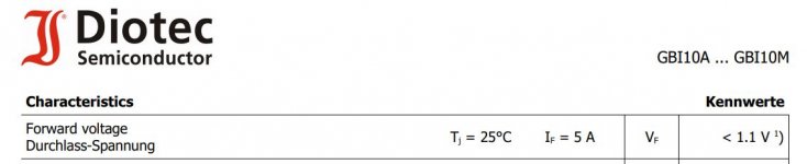
The choice of voltage for the power transformer must be chosen taking into account the voltage drop on the rectifier bridge mainly, but also on the resistive elements.
The amplifier can also be powered with 15vdc without problems. 😀😀😀
I would recommend that they be powered over 24vdc.
The amplifier can also be powered with 15vdc without problems. 😀😀😀
I would recommend that they be powered over 24vdc.
Attachments
Last edited:
Besides csample, has anyone tried a single power unit, even if the original article proposes a transformer with 2 coils?
Not sure to get it. It's always interesting to see how different people made different builds/choices from the same scheme: increased capacitances, single versus double power supplies, several boards versus all on one board, etc.).
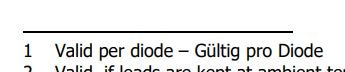
Regarding the pcb post #244, looks like the junction/connection between R1-R2-R4 is missing withing the right channel.
Still wondering how the inputs-outputs are connected in this board (one ground per signal, or one ground per input/output, or grounds only for outputs...?).
🙂
Regarding the pcb post #244, looks like the junction/connection between R1-R2-R4 is missing withing the right channel.
Still wondering how the inputs-outputs are connected in this board (one ground per signal, or one ground per input/output, or grounds only for outputs...?).
🙂
Show me in a drawing.Regarding the pcb post #244, looks like the junction/connection between R1-R2-R4 is missing withing the right channel.
Especially for you I will put more GND connections. 🙂🙄Still wondering how the inputs-outputs are connected in this board (one ground per signal, or one ground per input/output, or grounds only for outputs...?).
🙂
--------------------------------------------------------------------------
This will be the final version. But I'm not quite sure.
I rushed a bit with attaching the files without paying attention to certain details. I will ask a moderator to change the files with some correct ones.

Attachments
Last edited:
Hi again,
Here is a crop regarding what I was saying above.
On the left side, there is a (blue) connection between R1, R2 and R4.
On the right side, R2 and R4 are connected together, but no connection to R1.

Regarding the ground connections, thanks, it's clear now. Will have to take care about loops though 🙂
Here is a crop regarding what I was saying above.
On the left side, there is a (blue) connection between R1, R2 and R4.
On the right side, R2 and R4 are connected together, but no connection to R1.
Regarding the ground connections, thanks, it's clear now. Will have to take care about loops though 🙂
I think this is more appropriate. Single connection for GND signal. 
I also corrected the connection between the resistors.
I also corrected the connection between the resistors.
Attachments

Last edited:
That's all. I hope there was no mistake.
Good luck!!!!
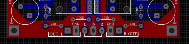
I'm asking a moderator to delete the files from the 244 post because they are wrong. Thanks.
corrected files // 244 post //
I have corrected the files posting 244. Maybe I will make some boards at the factory but after going over this situation with the virus.
According to the promise I will also draw the power supply.
I have corrected the files posting 244. Maybe I will make some boards at the factory but after going over this situation with the virus.
According to the promise I will also draw the power supply.
Attachments
Wondering if there is a recommended value for the input cap.?
The original build recommends 4.7µF, but fine results were obtained too with 2.2µF.
How is the value of this component supposed to affect the sound quality?
The original build recommends 4.7µF, but fine results were obtained too with 2.2µF.
How is the value of this component supposed to affect the sound quality?
Wondering if there is a recommended value for the input cap.?
The original build recommends 4.7µF, but fine results were obtained too with 2.2µF.
How is the value of this component supposed to affect the sound quality?
Hello,
with both values the lower bandpass limit will be below human sensitivity: my advice is to use the best quality component (with reasonable values) you have in your drawer.
Ciao,
Marcello
Size has to be taken into account too for those who already got their case 😉
Standard Wima MKP10 is one option; Audyn are bigger and might not always fit.
Standard Wima MKP10 is one option; Audyn are bigger and might not always fit.
Wima MKP is very good.
For other exotic options it is recommended to mount them on the housing, to see everyone with the price attached.
I used Miflex 2.2uF axial.
For other exotic options it is recommended to mount them on the housing, to see everyone with the price attached.
I used Miflex 2.2uF axial.
According to the original publication, Q2 (IRF610) must be matched to ensure the same gain between the two channels. Which parameter should be checked/matched for Q2 if using a transistor tester instead of the proposed matching circuit?
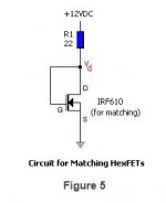
🙄🙄Circuit for matching HexFETs. by Marcello Pellerano
Figure 5
The “active side” HexFETs (Q2) must be matched to ensure the same gain between the two channels (the current source gain can be set by the trimmer (this is another difference respect to the current sources in the Aleph amps, which constrain to select all the devices, not only the “signal” ones).
I built a simple matching circuit shown in figure 5. The bias current is 360mA (calculated as Ibias = (V1 – 4)/R1). It may be regulated with a correct value for the power supply voltage (12V in this case) and for the R value. The HexFET component should be thermal stabilized (a couple of minutes or so) and heatsinked during this test. The selection parameter is Vd, and its value is around 4V. For matching the HexFETs, I think that 0.1V tolerance is plentiful. Devices matched to a few fractions of volt can be achieved, in my opinion, by buying ten or fifteen pieces, and make the matching among these. I bought 50 pieces and found, if I recall right, many 4.17V units.
Attachments
Hi knauf1919,
Thanks for the reply and for the fig/method from the original publication.
Now that I have a transistor tester I was wondering if it's possible to match Q2 with the tester instead of the circuit shown in fig5, in order to avoid the thermal stabilization and the heatsink. If the only way is the matching circuit in fig5, let it be 😉
Hi knauf1919,
If the only way is the matching circuit in fig5, let it be 😉
In this case it is the most suitable test. Do it, it's simple.


- Home
- Amplifiers
- Pass Labs
- ZEN-like headphones amp