I think that would be an interesting circuit. If I read therdk845 said:
I have been vigorously looking entire diyaudio forum for any information on build of Zen I/V or D1 for PCM 1794.
datasheet correctly, the output is biased at about -6mA
centerpoint and would like to see a low impedance load.
This suggests that a single-ended Common-Gate device
could be biased through the DAC directly given an
appropriate Gate bias voltage.
😎
I am still trying to figure how to bias a single-ended common-gate device through the dac directly, this is what I came up with (please don't laugh if it is completely wrong). Would this work?
As a simplified topology it is workable. Presumes that the DAC biases the Fet
as desired, but you can supplement that if needed, Probably want to have a
resistor in series with the Gate and output to suppress parasitic oscillation.
as desired, but you can supplement that if needed, Probably want to have a
resistor in series with the Gate and output to suppress parasitic oscillation.
Thanks Papa! I am honored to get a reply directly from the one and only 🙂As a simplified topology it is workable. Presumes that the DAC biases the Fet
as desired, but you can supplement that if needed, Probably want to have a
resistor in series with the Gate and output to suppress parasitic oscillation.
Again, my knowledge on circuit design is too limited to know how to complete the circuit. I have added the resistors in series as suggested, and also some power supply filter that I see featured in D1 and other circuits. Is this good enough for actual implementation?
Best regards
Liu
PM1796, as stated in the schematics, is 3.5mA DC current sink, plus +/-2mA signal.
Happy New Year to you, Nelson,
Patrick
Happy New Year to you, Nelson,
Patrick
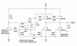
The idea is very clever, I like that.
But you want to have 0V DC and a low impedance at the DAC current output.
That means that you have to use a high-transconductance JFET, such as 2SK3557-6.
Those, unfortunately, have Idss much higher than 3.5mA.
That also means that you need an adjustable negative gate voltage to set input to 0V.
And even then, the Yfs at 3.5mA is somewhat low, equivalent to ~60R input impedance.
But performance is great.
Only thing to criticise, if any, is the poor PSRR to the top rail.
And the need of a coupling cap.
But that can be solved using a current mirror.
This is how I would do it in practice.
The Zip file contains Spice files ready to run.
Very nice performance in sim.
Patrick
.
Attachments
Wow. That is nothing short of amazing! Thanks a ton Patrick. It will probably take me ages to arrive at that if I were to learn to do it step by step! I would need to study it carefully to understand how it works though 🙂 . Also a follow up question on the Vs: what would be the recommended rail voltage: would +-18V be OK?
Thanks to Papa for providing the initial concept. I am always inspired by how you come up with brilliant ideas to maximize the advantage and special characteristics of components.
Next would be to study how to draw PCB with KiCAD and try to draw a draft.
Thanks to Papa for providing the initial concept. I am always inspired by how you come up with brilliant ideas to maximize the advantage and special characteristics of components.
Next would be to study how to draw PCB with KiCAD and try to draw a draft.
So member smms73 tested the PCM1794 can live with 100R at the output.
Probably 60R is also OK for the 1796.
https://www.diyaudio.com/community/threads/testing-the-pcm1794.221743/post-3205161
Patrick
Probably 60R is also OK for the 1796.
https://www.diyaudio.com/community/threads/testing-the-pcm1794.221743/post-3205161
Patrick
Open the Zip file and run LTSpice.
It has all the information you need.
And you need a very low noise power supply.
LT3045/3094, or Didden Super Regulators.
Patrick
It has all the information you need.
And you need a very low noise power supply.
LT3045/3094, or Didden Super Regulators.
Patrick
This circuit only works if the DAC is sinking current.
I am not sure whether that is the case with the PCM1796.
No experience with that chip.
So this is the first thing you should find out.
TI seems to say that it is sourcing and not sinking :
https://e2e.ti.com/support/audio-group/audio/f/audio-forum/890747/pcm1792a-sinking-or-sourcig
That means you have to flip the whole thing upside down and use PJFETs.
Patrick
Last edited:
Ok, Patrick. Thanks for the further info. I guess I have a lot more homework to do before being able to reach the actual implementation. I am sure I will learn a lot more along the line, and I look forward to that.
Best regards
Liu
Best regards
Liu
Patrick, you are super kind! I can't tell you how much I appreciate the help!
As for the fact finding about PCM1796, from what I found, it seems that most people agree that it is sinking current rather than sourcing current. https://electronics.stackexchange.com/questions/189998/direction-of-dac-output-current. As mentioned by the guys in this forum, and as stated in the datasheet, the center current is -3.5mA, and the negative sign indicates the direction of the current flow i.e. into the current output pin rather than out from it. With that information, I would probably start on a bread board with the current sink version and see whether it works correctly with the dac.
To confirm it before connecting, I guess I could connect the positive output pin in series with a 100 ohm resistor to ground and check the voltage, and if it is negative, then I can be sure that the chip is sinking current, am I right?
Also, regarding the 10k trimpot adjustment, I would have to complete the adjustment of the negative gate voltage and get a 0V at the input, power down and then connect the dac chip, right?
Best regards
Liu
Attachments
This will be the last post from me on this subject.
It is an idea you posted yourself, so you should know how.
And I do not have time to nurse you through this.
Yes. But I would bet it is positive.
Yes, but you need to provide a constant current of 3.5mA to emulate the DAC output DC current (whether sourcing or sinking).
And the rail voltage has to be regulated or your DC adjustment will drift.
And you need to readjust once the chip is connected, because it might not source or sink exactly 3.5mA.
Success,
Patrick
It is an idea you posted yourself, so you should know how.
And I do not have time to nurse you through this.
I could connect the positive output pin in series with a 100 ohm resistor to ground and check the voltage,
and if it is negative, then the chip is sinking current
Yes. But I would bet it is positive.
regarding the 10k trimpot adjustment, I would have to complete the adjustment of the negative gate voltage
and get a 0V at the input, power down and then connect the dac chip
Yes, but you need to provide a constant current of 3.5mA to emulate the DAC output DC current (whether sourcing or sinking).
And the rail voltage has to be regulated or your DC adjustment will drift.
And you need to readjust once the chip is connected, because it might not source or sink exactly 3.5mA.
Success,
Patrick
Since we are using 2SJ74 anyhow, you can replace the 4x 2SK209 with a pair of matched 2SK170BL.
Patrick
Patrick
Hmm....I am thinking about making a PCB that would give choices of opting for some or all of the above.
1. Traces to accomodate the J175 cascoding jfet + a jumper to short it out in case one prefers the non-cascoded version.
2. Traces to accomodate 4x TO92 jfets. If for some reason one prefers to use 4xSK209, he can just mount them onto a converter and populate them on the main PCB.
CLiu
1. Traces to accomodate the J175 cascoding jfet + a jumper to short it out in case one prefers the non-cascoded version.
2. Traces to accomodate 4x TO92 jfets. If for some reason one prefers to use 4xSK209, he can just mount them onto a converter and populate them on the main PCB.
CLiu
- Home
- Amplifiers
- Pass Labs
- Zen I/V Converter