Very nice circuit. I like it a lot better than the D1, but .....
1. Highish input resistance (> 10R) and capacitance ? Some DACs like PCM1704s might not like it.
1a. Highish output resistance especially if more gain required, but solvable by adding a JFET follower.
2. A pity you could not get rid of the coupling caps. Maybe a folded cascode ?
3. And how about a balanced version that has some extra distortion cancellation trick ?
Patrick
Last edited:
I am not home right now, so I cannot post a schematics. Also I have not been thinking about it for weeks, so this may not be ultimo version.
Take a PCM1704 with +/-1mA output as example. To get 2Vrms standard CD output, one would need to use 5.6k drain resistors for the JFETs. Somewhat high for driving cables, so a buffer maybe desirable. One can use a single ended JFET follower, or a complmentary one to go with the rest of the circuit. Input resistance is about 33R // 40R, i.e. around 17R.
But if we accept the complexity of a folded cascode to get rid of the coupling caps, we might even get away with lower rail voltages. Using 2SK2013 / 2SJ313 as cascode devices at say 50mA with the source at say +/-12V (gates at ca. +/-9.5V), we can even use +/- 18V rails. And the cascode would reduce input capacitance (so we can consider paralleling JFETs to reduce input resistance as well as noise) and improve PSRR. The output resistor is now reduced to a single 2.8k for 1 complemetary JFET pair, which can be placed at the output socket, or even at the end of the interconnect cable.
Mirror imaging will get me a balanced version, and if properly match they will cancel even harmonics.
Yes, I have a single ended, balanced version of this in the process of being built and tested, but I have not yet been able to come up with a means of cross coupling the 2 differential halves in any beneficial way.
Your comments ?
Patrick
Attachments
Last edited:
Great article. Thank you.
Now for the dangerous part. I assume (most dangerous word in engineering) that for a DAC chip like the PCM1794 that has differential current outputs, I would simply use 2 circuits per channel. Also, because the DAC chip puts out almost 8 ma of current, the 10 ma jfets would be sufficient.
If I needed single ended operation, I could convert it by the usual tricks.
Here is the data sheet for the PCM1794 focus.ti.com/lit/ds/symlink/pcm1794.pdf
Doug
Neat circuit! When I saw it I thought it looked familiar. I was doing some searching for common-base circuits for I/V about two days ago and this caught my eye. Notice any resemblance? 
Moving Coil Cartridge Head Amps
Moving Coil Cartridge Head Amps
i will definitely build this for my akm4396
No, you won't - ak4396 DAC chip features voltage output only...
sad to hear this
Don't be sad, it's excellent sounding chip as it is

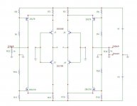
This is a quick & dirty schematics just to show the idea of a cascoded complementary JFET IV.
I hesistated to call it cascoded Zen IV, as it is more of a "Blowtorch IV".
Balanced DAC current is fed to the sources of the input jfets, whose gates are tied to ground.
R2,3,19,21 are bias resistors for the folded cascode MOSFETs (say 200R).
Conversion gain (I to V) is set by R22,24.
One may add additional electrolytic caps to parallel R5,6,16,17.
And R1/18, R4/20 can be replaced by constant current diodes for further improved PSRR.
The rails can now be quick a bit lower than +/-30V.
And the choice is not affected by changes in IV conversion gain and first stage bias.
So one can increase R22,24 (say to 2.4k) and use multiple JFETs in parallel without changing Vsupply.
When using JFETs in parallel, R2,3,19,21 wants to be reduced by N (no.of JFETs in parallel).
No coupling output caps, but consumes quick a bit more current.
Patrick
Attachments
Hello,
In the same way, I made, with the "UGS by CheffDeGaar" described here :
http://www.diyaudio.com/forums/pass-labs/86300-ugs-adventures.html
a Balanced I/U stage.
The schematic is here :

Here in my cd drive with ad1865 (non over sampling) :
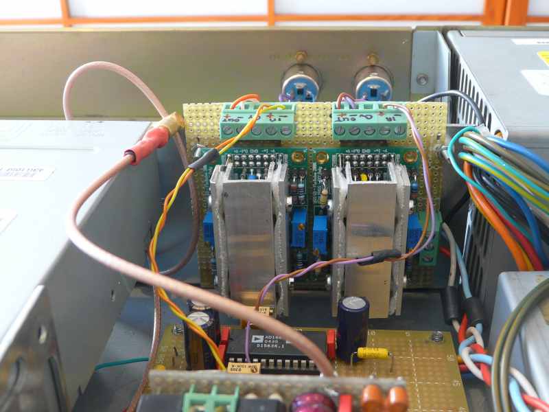
and the topic (in french, sorry) is here :
UGS, DAC, et Cie - TDG
Philippe
In the same way, I made, with the "UGS by CheffDeGaar" described here :
http://www.diyaudio.com/forums/pass-labs/86300-ugs-adventures.html
a Balanced I/U stage.
The schematic is here :
Here in my cd drive with ad1865 (non over sampling) :

and the topic (in french, sorry) is here :
UGS, DAC, et Cie - TDG
Philippe
I have used the D1 I/V for several years with great pleasure.
So the next pleasure might be this jfet I/V converter.
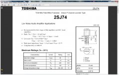
Just one thing makes me scratch my head, there are 30V on the drains
of the 2sj74, but the toshiba datacheet tells me a maximum drain gate voltage,
or breakdown voltage of just 25V.
I would like to use my +/- 30V supply from my D1 I/V converter.
Did someone allready tried this new circuit without killing the jfets?
Attachments
- Home
- Amplifiers
- Pass Labs
- Zen I/V Converter
