OK, finally I spotted the problem. Basically a Schrodinger cat problem. One return GND line was missing, so my measurement system was acting for it, so depending how I was connecting probes the thing was working or not. Once the connection was done in a solid way, everything went under control.
D.
D.
Just to avoid confusion, I was not using the original pcb from the evaluation kit.
The sound so far is very good, still could not move it to the living room, as I am missing the psu for the dac.
D
The sound so far is very good, still could not move it to the living room, as I am missing the psu for the dac.
D
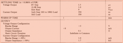
About Civ, I was thinking to go for the AD1865 with 1500 ohm 0.0022uF (cut-off 48kHz) and for the ESS9018 with 400 ohm 0.0022uF (cut-off 58kHz). Does it seems reasonable ?
Any specific type of capacitor recommended ?
D.
Any specific type of capacitor recommended ?
D.
The ES9018 has a much higher sampling rate. (Not sure if it upsamples automatically.)
So you can try 100kHz first, and see if there are still lots of HF noise left.
P.
So you can try 100kHz first, and see if there are still lots of HF noise left.
P.
The ESS also has his hen filters and on the scope there is no much left in reality, but it's worth to look again.
D
D
Hi all here.
As i am fiddling with a new "old" AD1856 i just bought from diyinhk, i also would like to make my own i/v stage for omitting the buildin opamp.
AD1856 R2R Isolated nonoversampling NOS Audio DAC with FIFO reclock V2 - DIYINHK
This dac i bought uses two AD1856 dac chip's, and datasheet states the following specs, which i think is important in my case.
+-3V or +-1mA output capability and so forth.
Eventhrough i read the article several times, i still find it hard to figure out what i have to build, and if it's possible at all with this dac? -Also i cannot find in thread if it's possible to use with an regulated 18vdc psu instead of using batteries? (I actually have an diyaudio superregulator in drawer 🙂)
About the transistors, i have a handfull of 2sj74bl, 2sk170gr, 2sk170bl, one 2sk389V and two 2sj109V.
Hoping that someone can guide me a little further thanks 🙂
Jesper.
Attachments
You can build a cen or sen, to your liking, but you have to use one battery per phase or channel. We use batteries to have the psu floating
D
D

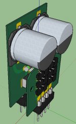
I/V, AD844 pin compatible, heatsink missing but mounting holes present.
Will use this one for DSC1 redesign.
JP
Sorry for the dumb question, but its a SEN derived?
did you try It already
great i/u OPAmp replacement
great i/u OPAmp replacement
I/V, AD844 pin compatible, heatsink missing but mounting holes present.
Will use this one for DSC1 redesign.
JP
Sorry for the dumb question, but its a SEN derived?
It's BF862 cascoded by J111 version
I have to replace my batteries. The old ones were 600 mAh but the new ones are 500 mAh. If I do not change Rch for the charging circuit I will then get C/33.3 instead of C/40 which is recommended. Anyone knows what effect that will have on the batteries? I am asking because it will take me a while to replace the resistors since my case is packed pretty tight so if it will not make a difference I would rather not do that.
Last edited:
This variant of the SEN I-V uses the available and inexpensive SMD BF862 jfet cascoded by J111, 3 in parallel ... and since we are doing overkill, let's go all the way and mirror balanced I-V circuits.
View attachment 593934
I'm using SMD film 0.1uF bypass caps but use a really high quality resistor at R3 and R7 attached at the output... thoughts on layout?
View attachment 593938
View attachment 593935
View attachment 593936
There are holes to allow a small finned heatsink to be placed over the 12 JFET array on each side of the board and tied in place with a cord.
Following this comes a similarly mirrored SK filter using Wurcer's discrete OPA (BF862 with hybrid BJT cascode)...
@jborden
I have a few questions.
- Can this be used with the es9018 (BufIII)?
-If yes, then how would you handle the DC ofset. Like its done in post #1883? http://www.diyaudio.com/forums/digi...-evolution-minimalistic-iv-converter-189.html
-What is the purpose of R2 and R8?
- Can this be used with the es9018 (BufIII)?
-If yes, then how would you handle the DC ofset. Like its done in post #1883? http://www.diyaudio.com/forums/digi...-evolution-minimalistic-iv-converter-189.html
-What is the purpose of R2 and R8?
I haven't worked with the es9018 but would handle DC offset as described. If I redo the layout it would be easy to provide this as an option.
R4/R8 were there from testing -- I leave them out
I also leave out Civ because the next stage has an input C -- would be redundant for my purposes.
For the es9018 or different DACs the big difference would be number of parallel jFets based on ldss. EUVL has described this both in the article and in this thread.
HI jborden.
Thanks for the reply.
Couple of more questions.
What is the input impedance in yore setup?
Regarding DC offset. Where would the DC adjustment go in your diagram? To the drain of J2 J3 and J9?
Thanks for the reply.
Couple of more questions.
What is the input impedance in yore setup?
Regarding DC offset. Where would the DC adjustment go in your diagram? To the drain of J2 J3 and J9?
impedance: 15k (see digital output section of signalyst dsc1)
dc offset: yes, the drains are tied to ground in my schematic (and the base SEN I-V).
Ground in the SEN (given its floating supply) is simply a 0v reference, but can be set as desired.
I'd recommend checking things in LTSpice 🙂
dc offset: yes, the drains are tied to ground in my schematic (and the base SEN I-V).
Ground in the SEN (given its floating supply) is simply a 0v reference, but can be set as desired.
I'd recommend checking things in LTSpice 🙂
Last edited:
- Home
- Source & Line
- Digital Line Level
- Zen -> Cen -> Sen, evolution of a minimalistic IV Converter