Hi I'm building an audio mux with volume control using a couple of digital potentiometers.
The digi-pots require the signal through its pot connections to be between GND and VCC which is 5v so I decided I will raise the audio input ground to 2.5V with an op amp or maybe an LM317 regulator.
I will connect the digi-pot as a regular potentiometer, the input at one end, the ground at the other and take the output between the wiper and ground only that the input and output signal ground to this digi-pot will be the 2.5V reference line. The audio signal is AC coupled and dc-shifted to the same 2.5V line.
SWITCHING:
I have several options to try to switch the input audio,
1) use a whole 4066 for each audio channel, that is one 4066 for the left channel & another for the right, that's for each input channel. Each channel is a "T", two switches in series, and the connection between them is connected through another switch to the 2.5V line. Adv: When I disconnect this channel, it looks like 100M ohm in series with another 100M input to output and 125 ohms to 2.5V between them. Disadv. takes lots of board space (not a big problem), cost doesn't matter.
2) use 4052 for all 4 stereo inputs, Adv. small board space but I need HELP here, I want to achieve the same effect of connecting the input to be disconnected with the reference line instead, if VCC is at 5v and VSS at 0, can I connect the VEE to the 2.5V or does it have to be below VSS?
3) use 4053 and switch the audio input with its reference; L, R & Gnd but still may need to connect VEE to 2.5V
Bear in mind that CMOS switches have non-linear resistance, which becomes more non linear at lower supply voltages. The impedance after the switch needs to be high enough to preserve waveform shape.
The supply for the switches must be at least equal to the input voltage range, preferably with some headroom. The switches will pass any DC level that is within the supply range. Therefore VDD has to be greater or equal to 5V and VEE needs to 0V or negative. Control signals remain at logic levels. VSS 0V for 4052.
The supply for the switches must be at least equal to the input voltage range, preferably with some headroom. The switches will pass any DC level that is within the supply range. Therefore VDD has to be greater or equal to 5V and VEE needs to 0V or negative. Control signals remain at logic levels. VSS 0V for 4052.
@spladski the impedance following the switch will be not be less than about 5K is that enough? And since VEE cannot be positive then I shall use the 4066 switch then.
@Fogonazo thank you but these are the switches I have and I do not plan on ordering by any means.
@Fogonazo thank you but these are the switches I have and I do not plan on ordering by any means.
With a CMOS switch, to get good linearity, you either need to load it with a very high impedance to prevent any voltage drop across the switch itself due to signal current, or load it into a virtual earth, also to reduce the voltage across the switch. The latter technique allows you to switch much higher voltages than the meager voltages allowed by CMOS, but the switch capacitance tends to de-stabilize a current to voltage converter amplifier, which will be the switches load.
The best plan is to convert the signal voltage to a current using a series resistor, switch it with the CD4000 switch and then load the switch output into the inverting input of a virtual earth amplifier. As long as you keep the capacitance on the low side, you can compensate for it with a capacitor across the VE amp's feedback resistance. Try to run the CD4000 switch with as high of a symmetric supply voltage as possible, probably ±7V. This will prevent odd leakage problems and will maximize the linearity of the switch.
The best plan is to convert the signal voltage to a current using a series resistor, switch it with the CD4000 switch and then load the switch output into the inverting input of a virtual earth amplifier. As long as you keep the capacitance on the low side, you can compensate for it with a capacitor across the VE amp's feedback resistance. Try to run the CD4000 switch with as high of a symmetric supply voltage as possible, probably ±7V. This will prevent odd leakage problems and will maximize the linearity of the switch.
You really need to obtain the datasheet for the device, which is readily available, to read the resistance linearity. The 4066 has a resistance change approaching 200 ohms at 5V supply. With a 5K load, there will be distortion, but only you can determine whether it is acceptable. It won't be HiFi.
Better performance using the max supply voltage with a ref voltage slightly below half rail. There are also better devices for 5V operation.
Better performance using the max supply voltage with a ref voltage slightly below half rail. There are also better devices for 5V operation.
About linearity, the characteristic to look for in the datasheet is "On resistance flatness" (0.2 Ω for DG451)
If you have stuff to trade... I have new SSM2402 and SSM2404 for quality audio switching. The point of switching sources is that it also needs to sound good 🙂
Not a single device with the ICs you mention sounds excellent as these ICs are not meant for the purpose.
Not a single device with the ICs you mention sounds excellent as these ICs are not meant for the purpose.
Another issue not mentioned here are glitches caused by charge injection during switching. These will be audible.
Next issue are total fails after latchup.
Next issue are total fails after latchup.
One option I can see is to use a JFET opamp after the switch. This could have a 1M ohm input impedance in a voltage follower configuration and act as buffer for the 5K load.
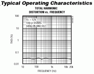
The MAX4066 claims to have only 45 Ohms at 12V supply, and 0.03% distortion, all better than the standard 4066s - maybe that is worth a try?
I had a look at the datasheet.
Their 0.03% THD is meaningless, there is no relevant information about conditions particularly the load impedance.
This figure is a bait to audiophile more than a spec.
A meaningful figure is the 4 ohm flatness that does relate to THD.
Their 0.03% THD is meaningless, there is no relevant information about conditions particularly the load impedance.
This figure is a bait to audiophile more than a spec.
A meaningful figure is the 4 ohm flatness that does relate to THD.
Douglas Self discusses at length the use of MUX in his small signal book. The best implementation thd wise uses one 4066 per channel in conjunction with an inverting opamp. You can get most of the discussion in the preview of the book on google books: Small- Signal Audio Design - Douglas Self - Google Livres (search 4066 and then scroll down to fig 16.17)
It goes like this:
after the input resistor, tie one switch to ground to shunt the signal when unused, put two switches in parallel going to the opamp inverting input and use one switch to invert the control signal.
It goes like this:
after the input resistor, tie one switch to ground to shunt the signal when unused, put two switches in parallel going to the opamp inverting input and use one switch to invert the control signal.
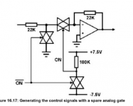
With better switches (and opamp), you could try to double up the shunt gate rather than the serie one, which would allow to reduce the value of the resistors, improving noise performance without compromising the "offness" and the distortion of the setup.
- Home
- Source & Line
- Analog Line Level
- Yet another mux, 4052, 4053 or 4066?