Have to agree - reflow usually does its own magic (and I mean usually...)Also - reflow my friend! Doesn't matter if you can't see the pins - you can still solder them.
E
I don't see the need for an additional heatsink; by adding more layers than are necessary you're just going to reduce overall thermal transfer.
However if you were going to package the device like this - I'd want to use 2oz copper, to cope with the current, and I would use an epoxy specifically designed for thermal transfer such as Arctic Alumina Adhesive. (the silver version, while nonconductive, is slightly capacitive.) This would definitely make a more robust device for non-permanent installations. 🙂
However if you were going to package the device like this - I'd want to use 2oz copper, to cope with the current, and I would use an epoxy specifically designed for thermal transfer such as Arctic Alumina Adhesive. (the silver version, while nonconductive, is slightly capacitive.) This would definitely make a more robust device for non-permanent installations. 🙂
but did you do that on such device as this and on home made pcb (I can already see that this is not on option, and since there are some really cheap companys that do it)Opto would be fine too. 🙂
Also - reflow my friend! Doesn't matter if you can't see the pins - you can still solder them.
While doing home-grade reflow on a device like this may be possible, the PCB production is indeed not something you could get away with doing at home.
Fortunately like you say there are a plethora of companies willing to do very cheap board production - especially in quantity, as we now see with the O2 amplifier boards. I'm looking into this as we speak, as many of these companies offer assembly services too I'm hopeful that we could get the whole thing produced professionally.
Fortunately like you say there are a plethora of companies willing to do very cheap board production - especially in quantity, as we now see with the O2 amplifier boards. I'm looking into this as we speak, as many of these companies offer assembly services too I'm hopeful that we could get the whole thing produced professionally.
homemade or not
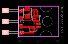
Meanwhile back at the ubermosfet, here's a view showing that there's indeed enough space in a TO-247.
Don't look at the layout, also with this placement there's no way to get a tight fit from mosfet to copper tab.
E
I would outsource it to a local assembly house. I'm currently in Italy and have good contacts from my day job. However, the PCB would have to be panelized, and depending on quantities, someone would have to figure out a more rational, easy and reproducible way to mount the heatsinks...but did you do that on such device as this and on home made pcb (I can already see that this is not on option, and since there are some really cheap companys that do it)
Meanwhile back at the ubermosfet, here's a view showing that there's indeed enough space in a TO-247.
Don't look at the layout, also with this placement there's no way to get a tight fit from mosfet to copper tab.
E
Attachments
where in Italy are you now?
well I guess once all will be figured out, component should be good for anything, not just this amp
well I guess once all will be figured out, component should be good for anything, not just this amp
Asti, (tele)commuting to Varese where the EMs are.where in Italy are you now?
E
...means our suppers were ready at about the same time 😉aha, near Milano... not that far away from me
Let's see if I can post the revised amp schematic later tonight.
E
I don't know about that, but no wonder you are on the net at such hours, now I know why 😛...means our suppers were ready at about the same time 😉
so you all like the eGaN fet 🙂
I think the best way to use them is to make a little module with 2 fet and a driver (for example the LM5113) and a decoupling capacitor, in that way we have all the high current nodes in the same place, and is easier to deal with the parasitic inductance.
The module can be made from a aluminum base pcb like this
Aluminum PCB | Metal Clad PCB (MCPCB) | PCB Products | Amitron Corporation
Sorry I don't understand "interleaved" in the context.
E
Interleaved is a technique to minimize leakage inductance in transformers to extend the high frequency of a transformer, it consist in placing a primary then a secondary then a primary again... . some audio transformers have like 10 primary's and 10 secondary's interleaved. but for a sub-woofer we only need that the primary has the inductance necessary.
I personally like transformers in audio.
hope the explanation is clear enough
Understood, thanks. Somehow I was stuck in "220V mains"Interleaved is a technique to minimize leakage inductance in transformers to extend the high frequency of a transformer...hope the explanation is clear enough
E
Ok, so if we include the bootstrap for the high side, that would be a 6-pin module?...I think the best way to use them is to make a little module with 2 fet and a driver (for example the LM5113)...
The module can be made from a aluminum base pcb
Funny, just today I was talking with a friend at a company manufacturing thick-film hybrids (usually on ceramic PCBs) and he suggested alu-cored PCBs also.
E
Yes, that's right, a 6 pin module.
your proposal of using the zxgd3002 is very good , we need a way of using conventional mosfet drivers with the eGaN FET.
I just don't like the idea of using separate mosfet, because of the parasitic inductance's.
your proposal of using the zxgd3002 is very good , we need a way of using conventional mosfet drivers with the eGaN FET.
I just don't like the idea of using separate mosfet, because of the parasitic inductance's.
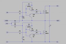
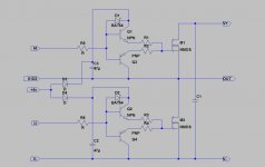
I think we need something like this, its like elevator driver with the add of a input resistor and a clamp diode for preventing that the npn transistor saturate.
A 8 pin module, but it is best to use more pins for the V+ V- and OUT for current and mechanical stability of the module .
A 8 pin module, but it is best to use more pins for the V+ V- and OUT for current and mechanical stability of the module .
Attachments
ubermosfet slash two
Something like this, guys? Two granmas? Anything else? No body diodes?
Now the challenge is to turn this into a one-sided PCB, no jumpers😀.
I wonder if the mosfets should have heat carried away from their substrate (ie upper) side as well, eg with a spring clip. I could have a thermal sim done once the layout is here.
I like the aluminum base PCB because you could directly screw it onto a heatsink.
On the upper side maybe conformal-coat it (in black, so that non-forum-members won't have a clue 😀)
E
PS the amp schematic is in the mail...
PPS parasitic inductances are like flea on an otherwise good dog...
Yes, that's right, a 6 pin module.
your proposal of using the zxgd3002 is very good , we need a way of using conventional mosfet drivers with the eGaN FET.
I just don't like the idea of using separate mosfet, because of the parasitic inductance's.
Something like this, guys? Two granmas? Anything else? No body diodes?
Now the challenge is to turn this into a one-sided PCB, no jumpers😀.
I wonder if the mosfets should have heat carried away from their substrate (ie upper) side as well, eg with a spring clip. I could have a thermal sim done once the layout is here.
I like the aluminum base PCB because you could directly screw it onto a heatsink.
On the upper side maybe conformal-coat it (in black, so that non-forum-members won't have a clue 😀)
E
PS the amp schematic is in the mail...
PPS parasitic inductances are like flea on an otherwise good dog...
Attachments

Last edited:
Sorry for the overlap.I think we need something like this, its like elevator driver with the add of a input resistor and a clamp diode for preventing that the npn transistor saturate.
Are you thinking of discrete BJTs or are they to simulate the driver chips?
The additional two pins make sense.
E
- Home
- Amplifiers
- Class D
- YAUSA - Yet Another Ucd (S?) Amp with SiLabs Chip