if you use the amplifier inside the speakers , like a sub-woofer amplifier for example , you can use the amplifier without the output transformer, i think it can be done, i even think is a very good solution for sub-woofer as the input transformer don't need to be interleaved.
Go for it.
Go for it.
I would be delighted to follow your calculations. One of the nice things about DIY is that it is very much an experimental endeavour. IOW let's see (and touch, and get burned 🙂) ....we can not use several nf Ciss mosfet with this drivers.
By the time this project is done, even vaporware may have turned into real hardware! 🙂 I like the Infineon. Also, there are a few IR twins (2 in one TO-220) which look good, for lower power use.where you going to buy this mosfet, it seems than nobody supply them yet
E
Last edited:
I would be delighted to follow your calculations.
E
No need for calculations 😎
They already have done that for you, just see the page 19 of the si824x datasheet.
And if you want to do your one calculations they have the equations on page 18. 😉
One paper that i find very good in that subject is this :
http://www.ti.com/lit/ml/slup169/slup169.pdf
The IR twins have a problem the up mosfet have a low source inductance as is direct connected to the drain of the low mosfet, and this source inductance (10nH on TO220) are important as they limit di/dt, and you need a low di/dt if you want to minimize the dead time without the risk of destroying
 the mosfet , i think the to220 version of this mosfets are better
This fets are the best on the market:
EPC2010
200Vds, Rds 25mohm ,Qgt of 5nC , and no diode Reverse Recovery Charge
They are made from Gallium Nitride, the next big thing,
they are distributed by Digi-Key,
Almost perfect... the problem is the package 🙁
man that thing is a bit to small for diy, for most people even resistor of this size would be a problem, let alone several connecting case like this, kinda like BGA. I know size matters, but this is not for diy
what about demo board, and making it into amp, on desktop should be fun to see what can be done
http://epc-co.com/epc/documents/schematics/EPC9003_schematic.pdf
http://epc-co.com/epc/documents/schematics/EPC9003_schematic.pdf
Now I wonder if these could be mounted into a regular package, maybe TO-247. MmmmhI know size matters, but this is not for diy
 let's see...
limited gate drive
Thank you smms73, that's very good reading.
So in essence we mitigated one problem (dissipation on VGD) but highlighted another one (limited gate drive capability).
This in turn limits the present circuit on the higher power end.
How about using a complementary pair as post-driver stage, in the style of this?
Thanks
E
One paper that i find very good in that subject is this :
http://www.ti.com/lit/ml/slup169/slup169.pdf
Thank you smms73, that's very good reading.
So in essence we mitigated one problem (dissipation on VGD) but highlighted another one (limited gate drive capability).
This in turn limits the present circuit on the higher power end.
How about using a complementary pair as post-driver stage, in the style of this?
Thanks
E
I would skip the 247 and only look at 220, even by doing this you would hurt performance a lot, but still better then 247Now I wonder if these could be mounted into a regular package, maybe TO-247. Mmmmh
Eval board costs 95$ +/- other things, one could try and make amp out of it, all I think you need it pwm and LC on output (to see if this fets are really any good)
Only problem I see now is the price of 10$ for one fet and size of this damn thing, first one could be swallowed, but going around 2nd one is much harder, but... some say that... (Do you know where is this taken from? 🙂) ... it could be still, I have hot air station, solder paste, but no profi PCB made, only home made...
Last edited:
This would work, in fact I use ZXGD3002E6 on my two amps, take a lot of load of the IRS, and note that they are BJT's, would be even better if they were mosfets. Note this: they do use this kinda drives on their eval boardThank you smms73, that's very good reading.
So in essence we mitigated one problem (dissipation on VGD) but highlighted another one (limited gate drive capability).
This in turn limits the present circuit on the higher power end.
How about using a complementary pair as post-driver stage, in the style of this?
Thanks
E
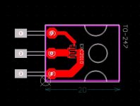
EPC2010 in a TO-247 package
In practice, the substrate would have to be glued on a metal slug, and everything encapsulated in epoxy...
(and the pinout reversed 😀 )
Come to think of it, there's enough real estate left for my grandma (AKA driver, gate resistor, bootstrap cap).
To be continued...
E
Just to get an idea of the proportions, here is the EPC2010 in a TO-247 package...I know size matters, but this is not for diy
In practice, the substrate would have to be glued on a metal slug, and everything encapsulated in epoxy...
(and the pinout reversed 😀 )
Come to think of it, there's enough real estate left for my grandma (AKA driver, gate resistor, bootstrap cap).
To be continued...
E
Attachments
what about with 220? inductance of leads is killing you hereJust to get an idea of the proportions, here is the EPC2010 in a TO-247 package...
In practice, the substrate would have to be glued on a metal slug, and everything encapsulated in epoxy...
(and the pinout reversed 😀 )
Come to think of it, there's enough real estate left for my grandma (AKA driver, gate resistor, bootstrap cap).
To be continued...
E
ubermosfet
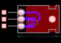
Meanwhile here's a peek at grandma 😀 What do you say luka? And smms73?
Mind you it's now a 4-pin affair.
TO-220 Coming Real Soon Now.what about with 220? inductance of leads is killing you here
Meanwhile here's a peek at grandma 😀 What do you say luka? And smms73?
Mind you it's now a 4-pin affair.
Add to these a microscope, a stencil with rake, a toaster, and you're in business! 😛I have hot air station, solder paste, but no profi PCB made, only home made...
Attachments

Nice fet - don't be put off by tiny parts. I'm currently investigating the possibility of having a breakout produced with nice through-hole pins to let us use this part. 🙂
Also just FYI - it's passivated with solder bars; it can be reflowed straight onto a PCB without adding any more solder, just need the land pattern right.
Also just FYI - it's passivated with solder bars; it can be reflowed straight onto a PCB without adding any more solder, just need the land pattern right.
yea this look ok, but how in the world would you do that?
ok make what, pcb the size of 220 or 247, and solder everything on that? and epoxy it to what, tab of 220 or 247?
ok make what, pcb the size of 220 or 247, and solder everything on that? and epoxy it to what, tab of 220 or 247?
mains-powered
E
Sorry I don't understand "interleaved" in the context. Another thing, I believe the input signal wires would need to be isolated from the rest, so the input stages, up to the gate drivers, would be powered from a (admittedly, small) galvanically isolated supply.if you use the amplifier inside the speakers , like a sub-woofer amplifier for example , you can use the amplifier without the output transformer, i think it can be done, i even think is a very good solution for sub-woofer as the input transformer don't need to be interleaved.
Go for it.
E
why do you think signal would need to be isolated? I never seen a need for thisSorry I don't understand "interleaved" in the context. Another thing, I believe the input signal wires would need to be isolated from the rest, so the input stages, up to the gate drivers, would be powered from a (admittedly, small) galvanically isolated supply.
E
I would have to agree - however a small signal trafo on the input is no big deal, and I have access to some lovely 1.5kv medical-grade isolated 12v supplies. 🙂
So am I right that the only issue is a human electrical safety risk with the output?
And yes - I would produce a PCB the size of some common package. Though no epoxying to anything would be needed - the die would be on the "back" of the device; in such a way that you can clamp it directly to a heatsink the same way you would a normal transistor.
For a mosfet it might seem small - but it's actually a fairly large part on the scale of common SMD components. This would translate to a "1406" size device (140 mils x 64 mils), and parts as small as 0806 or 0604 are possible to assemble by hand.
Last edited:
instead of trafos, I would if I would need to use linear opto
yes 0805 are still easy, but here we are talking about 7 or how many pins and you can't get to them
yes 0805 are still easy, but here we are talking about 7 or how many pins and you can't get to them
Opto would be fine too. 🙂
Also - reflow my friend! Doesn't matter if you can't see the pins - you can still solder them.
Also - reflow my friend! Doesn't matter if you can't see the pins - you can still solder them.
Luka,yea this look ok, but how in the world would you do that?
ok make what, pcb the size of 220 or 247, and solder everything on that? and epoxy it to what, tab of 220 or 247?
here's a stab at the EPC2010 on a TO-220. Nothing particular really. Bluefusion also has this in mind but without heatsink I believe.
Yes, the PCB would be the same size as a TO-220.
For the tab/heatsink I would choose copper in the same form factor as the TO-220 (and the PCB). Then, use epoxy glue, enough to cover all of the area, and immediately squeeze the two parts together with a laundry clip (preferably a strong one) taking care to keep the PCB (the mosfet substrate) tightly parallel to the copper. That won't be easy, so you want to mount a few spacer components approximately the same height as the mosfet chip on the PCB corners, before glueing. Maybe 0603 or 0402 resistors?
Once the thing is hardened you can deburr, make it look nice and post a pic here 😎
One more thing: I'd use a 1mm or 0.8mm thick PCB.
Also, ideally the epoxy should be one with good heat conduction.
E
Attachments
Last edited:
- Home
- Amplifiers
- Class D
- YAUSA - Yet Another Ucd (S?) Amp with SiLabs Chip