Here is a non-switching output stage that I invented. Nice and simple.
That's the Barry Thornton (SAE) circuit I was referencing,
clever boots.
😎
yeah, yeah, that's it!
wonder what he's doing now, anyways ...
mlloyd1
wonder what he's doing now, anyways ...
mlloyd1
That's the Barry Thornton (SAE) circuit I was referencing,
clever boots.
😎
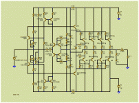
by homemodder - Discussing a circuit without schematic is kinda difficult so here is the full schematic for those interested.
Thank you, thank you , HM. I like this one (NS OP stage) I have the H.C.A. (fancy.. as yamaha calls it ! 🙂 ) running in place on my supersym LT simulation. I will finalize it soon and post. This seems to be a much better solution than any of the tanaka NS OP's or the "krill". I'm off and running with it.
😎😎
OS
Barry Thornton: US pat. 4160216.
Practically, every manufacturer had "non-switching" patent in those years.
Practically, every manufacturer had "non-switching" patent in those years.
Last edited:
wonder what he's doing now, anyways ...
Last time I talked to him he was an electronics rep down in
Arizona or New Mexico.
😎
This seems to be a much better solution than any of the tanaka NS OP's or the "krill". I'm off and running with it.
I wouldn't think anyone here would still consider the Krill after the trashing it took here.
Barry Thornton: US pat. 4160216.
Practically, every manufacturer had "non-switching" patent in those years.
In most cases I must pay for download patent pdf documents. Here a weblink for free download without registered:
http://www.patentretriever.com/cgi-bin/GetURL.cgi
to get this patent, please fill in exactly the follow:
us4,160,216
An additional weblink for free download without registered:
http://www.pat2pdf.org/
The good known patentarchive
http://www.patentstorm.us/patents/4160216.html
is only for registered users.
Hegglun fig 6a... MOSFETS strapped as diodes. Push and pull both abuse N-CH
as every 2 terminal diode is automagically quasi-complimentary... I guess these
MOSFET diodes had the square law curve he wanted? Seems a whole lot of FWD
voltage drop compared to a Schottky... I don't know the curve of a Schottky is
square in any special way, only that it has a low forward drop and seems to work
better than leaving non-linearity to whim of the output devices...
Pentode 6L6 had square law curves (read: OHSchade Beam Power Tubes, RCA).
I think square law distortion cancellation was old news and well known at the
time of Hegglun's paper. Just maybe not previously exploited in Solid State...
Last edited:
That's the Barry Thornton (SAE) circuit I was referencing,
clever boots.
😎
I figured it wouldn't be new. Anyway, he can take credit for the circuit; it introduces a non-linearity that is worse than the one it removes. 🙂
By steve dunlap - I wouldn't think anyone here would still consider the Krill after the trashing it took here.
My brother steve... now they can pick on me... 😀
I am impressed. The yamaha circuit , while looking complicated , works really well. I tried it at all frequencies (100 , 1k , 10k+), the plots look VERY consistant and it is VERY stable. (plot attached)
I just have to figure out how it is thermally compensated and how to tweak both the actual Xover point and the non-switching point. I am impressed that I got the plot below the FIRST time. For those interested , the .ASC is in {HCA_OPstage.zip} also included below... I like IT !! 😎
OS
Attachments

Last edited:
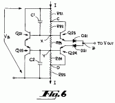

I'm not infringing ,am I .. papa ?? (maybe on yamaha 😛 )
By nelson pass - Looks familiar...
Last edited:
Looks familiar...
to get the complete document from Nov. 30, 1976 go to
http://www.patentretriever.com/index.html
and fill in
us3,995,228
Last edited:
I'm not infringing ,am I .. papa ?? (maybe on yamaha 😛 )
Long expired, but anyway Glen is spot on and I still don't get it. The extra diodes switch completely and are directly in the signal path (voltage-wise). The first circuit has far worse crossover distortion than a straight EF biased at the same level. The patent title is simply wrong. The author takes the fact that the output devices always have at least 100mA in them as a "good" thing in a completely abstract sense. There is not a single measurement of the simple input to output transfer function presented.
Just an idea, what if we used the body diodes of (fast) mosfets to block the "wrong direction" current and turn the fets on/off as required, by sensing the drop accross the emitter-Rs (and connecting the CCS's directly to the emitters)?Long expired, but anyway Glen is spot on and I still don't get it. The extra diodes switch completely and are directly in the signal path (voltage-wise).
- Klaus
Glen,
Don`t be sad, it causes a severe form of hyperbolic conversion distortion.I figured it wouldn't be new. Anyway, he can take credit for the circuit; it introduces a non-linearity that is worse than the one it removes.
😛😀By Lumba Ogir - Don`t be sad, it causes a severe form of hyperbolic conversion distortion.

I now agree. For the added complexity , I saw no great reduction in higher order harmonics with this OP stage. In fact , my present self type 3 triple outperformed it with half the component count despite the fact that it does switch (gracefully).
This conclusion was made only by simulations/FFT's , but the HCA is very similar to the JVC and technics IC bias stages ("super A"). I do have my old JVC with "super A" and it sounds good , but not any better than my DIY creations. Still , an interesting circuit.

OS
The MX-10000 circuit looks like a bridge amplifier without overall NFB and consists basicly two operational amplifiers and two power buffers - one pure class A (low voltage supply) and one class AB (high voltage supply). The first stage is a complete independend voltage gain amplifier (55 times).
The output stage of this one drives
1) the class AB power buffer (the output of class AB power buffer goes to the positive speaker terminal) and
2) the inverted input of a summing amp about a 6K8 resistor (non inverted input of this summing amp goes to GND)
The output of this summing amp (ERCO amp = Error Correction amp) drives the second power buffer, that is the pure class A buffer (the output of this buffer goes to the negative speaker terminal and also to the inverted input of a summing amp about a second 6K8 resistor
So I have a mixed signal between an (more or few) undistorted signal version from the voltage gain stage output and a distorted (and inverted) signal version from the neg. speaker terminal at the inverted input from the summing amp.
I cannot explain, why Yamaha calls this technology so than the head line of this thread.
If I replace the pure class A buffer through a "ZEN" or other simple single ended topology and the class AB buffer through an simple power buffer with 30-50 mA idle current, I get interest possibilities for diy projects (together with appropriate OP amp models for the voltage gain and ERCO amplifier stages).
This goal from Yamaha was the same than that of Quad's current dumping topology and the main different to Quad 405 power amplifier is the serial mode of the correction amp - Quad choises a parallel mode like the EDWIN amp projects from the Geman magazine "elektor" arround 1970 - 1975.
If I have remove the WIN32/ConflickerC worm from my own personal computer I will upload the basic schematic of Yamaha MX-10000 for better understand.
Here now the simplefield schematic as PDF file from Yamaha's MX-10000. I don't mention two resistors, one from the output of class AB power buffer to the non inverted input of summing amp (ERCO amp = Error Correction amp) and one from there to GND.
Attachments
- Home
- Amplifiers
- Solid State
- Yamaha's Hyperbolic Conversion Amplification (HCA) Circuit