Shielded, Insulated?
You don't need to use insulated wire as long ad there is no risk of the jumper making contact with another trace.
I don't know what you're using but resistors are dirt cheap and their legs make good jumpers.
You don't need to use insulated wire as long ad there is no risk of the jumper making contact with another trace.
I don't know what you're using but resistors are dirt cheap and their legs make good jumpers.
resistor legs are what i've been usingShielded, Insulated?
You don't need to use insulated wire as long ad there is no risk of the jumper making contact with another trace.
I don't know what you're using but resistors are dirt cheap and their legs make good jumpers.
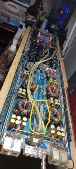
apologies for being repair illiterate but is it possible someone could explain what is happening in the highlighted area? There is a positive connection to the emitter of Q7, the base of Q7 is connected to the emitter of Q8, then the base of Q8 is connected to ground. Is the collector leg of both Q7 and Q8 connected to R60?
Attachments

Assuming that you understand the operation of an emitter-follower pair... The Zener simply limits the drive voltage to 10v (9.1v Zeners have also been used). The resistor allows a slight voltage drop from the output of the driver IC to the Zener voltage.
just to catch this up, the output fets have all been removed. I was able to see the traces on top of the board for the driver legs that are missing solder pads/via's, and would like to power test the amplifier. I had to remove 8 of these rods(not sure of the terminology of them) to see the traces and solder them well enough to be sure they are actually connected. Will the amplifier power up without these 8 rods? Or do i need to put them back in?
I've had to remove them twice now to work in the tight area where the drivers are. The board is mounted to a wooden frame as to minimize the flex to the board during flip overs
I've had to remove them twice now to work in the tight area where the drivers are. The board is mounted to a wooden frame as to minimize the flex to the board during flip overs
Attachments
Bussbars, jumpers? As long as you don't call them rails. For some people, everything is a rail.
It may not power up fully. Are they in parallel (connected together on the ends) or possibly two groups, a wire connecting the ends may be all you need. The connections may already be there and those are simply to increase the current capacity of the circuit.
It may not power up fully. Are they in parallel (connected together on the ends) or possibly two groups, a wire connecting the ends may be all you need. The connections may already be there and those are simply to increase the current capacity of the circuit.
So now the supply fets(IRFP064N) have been removed from the board because when i power tested my power supply was tripping and wouldn't power up. Even with the 064N's removed the power supply does the same thing, won't power up. The power supply is a AC DC 12V 50A 600W Regulated Switching Power Supply that I have mounted in a wooden box with stinger voltage meter and pioneer bluetooth headunit as my test bench.
My question is with the amp in the state that it is, where would be a good place to start troubleshooting? I'm sure there's a short somewhere, I'm just unsure on where to test for it and track it down. Thank you guys for any and all help provided. If any pictures are needed please let me know.

My question is with the amp in the state that it is, where would be a good place to start troubleshooting? I'm sure there's a short somewhere, I'm just unsure on where to test for it and track it down. Thank you guys for any and all help provided. If any pictures are needed please let me know.
Does it draw excessive current with only B+ and ground connected (no remote)?
If so, what's the resistance that you read across the B+ and ground terminals (nothing connected to the amp but your multimeter)?
Could you possibly have any solder bridges?
If so, what's the resistance that you read across the B+ and ground terminals (nothing connected to the amp but your multimeter)?
Could you possibly have any solder bridges?
Not seeing any current draw under either configuration. Test 0.4 ohms across + and - with only meter connection and haven't seen any solder bridges yet though still looking, there are so many points I want to be thorough. I'm going to remove the rectifiers to seperate the supply/output sections and test once more.
same results and now the rectifiers are removed. Power is still tripping so now i believe i'll pull the A1275/C3223 drivers too see if one of those might be shorted. They were ordered through digikey, same batch and installed brand new
not sure what those are, where would they be located and what type of encapsulation? I've made progress though, the center group of drivers I was having trouble locating the connection points for seems to be where the short was. After removing all 8 drivers the board does power up. It's an ugly spot to work with, I believe it might be the reason Kevin Mansky got so aggrivated with the repair.
You don't need to look for them if you found the short but... RP diodes are typically large cylindrical diodes. Sometimes multiple. Not all amps use them.
You need to make 100% sure that the connections to the drivers are absolutely rock solid. One intermittent connection can cause the entire supply to fail. Where traces are on both sides of the board, solder top and bottom.
You need to make 100% sure that the connections to the drivers are absolutely rock solid. One intermittent connection can cause the entire supply to fail. Where traces are on both sides of the board, solder top and bottom.
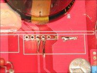
notice the 3 spots where there's no solder pad around the hole, i'm able to solder those locations on top of the board. Do they also need to be soldered on bottom?
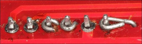
For the transistors that have damaged foil, scrape the solder mask back and tin the trace. Wrap something like the leg of a 1/8w resistor tightly around the transistor leg on the side with the trace and solder the wire down and to the leg of the transistor. Try to do it for at least 1/4" for each location where you have to use the wire. At least as far back as it takes to get to trace that's still bound to the board but at least 1/4".
Wrap like first image but solder on trace like the second image. These went through the board but the basics are the same.
Wrap like first image but solder on trace like the second image. These went through the board but the basics are the same.
Attachments
will do, looks like a very sturdy fix. Just hope I get the connections right cuz i'm not good at reading schematics. I still have the GZ4000d schematic you posted. I know what area on the schematic this driver group is but I don't understand the connection path
.png")
when i first removed the drivers the center legs were soldered on top of the board to a nearby trace

when i first removed the drivers the center legs were soldered on top of the board to a nearby trace
First, you MUST remove any carbonized material. If you don't, it's a fire hazard.
The PNP driver transistors have their collectors grounded. That's the most important connection.
For each NPN/PNPpair of drivers, their emitters are directly connected and their bases are directly connected.
The collectors of the NPN drivers go to a positive voltage source.
The emitters of each driver pair go to the gate resistors.
The bases of each driver pair get driven from the TLx94/ka7500.
from what you said in post 58, this is a small bmp i've put together of the connections. I'm aware all of these connections will not be on one side of the board, some will be on the bottom also. Do you see anything wrong in the connections? This is only so i'll know how and where the connections need to be made beings i can't read a diagram...but it's a work in progress

- Home
- General Interest
- Car Audio
- XXV Sampson power up issues