As I mentioned the boards are equipped with NDK oscillators (the waiting was long). Regarding GSGSGSGS you are correct, in terms of EMS, this kind of interface is better, but in terms of jitter according to me – no. The GSGSGSGS increases the capacity of the signal wire (almost double), this leads to slant fronts of the signal, which is precondition for bigger jitter in consequence of the non avoidable noises in the system.
Regards,
Joro
The best way to transmit a digital signal for maximum signal integrity is GSGSGS where each signal has its own return path. I don't know what you mean by increasing the capacity of the signal wire and slanting the front of the signal, but whatever it means it is incorrect.... Digital signals need a good return path, not having one will increase signal integrity problems such as jitter. The slanting of a signals front is the high frequency harmonic content of the square wave being attenuated, slowing the rise (and fall) times of the signal, this is not always detrimental to a signal.
Hi,
Standard flat ribbon cable has around 50pF capacity per meter, taking into account that we talk about GSG this capacity is doubled. For 10cm line this will lead to worse the rise/fall time with almost 1ns additional, as we have terminations resistors 33 ohm. This additional time is precondition to increase the jitter in this particular case. The increasing of the rise/fall time is not bad if we want to transmit only data, without taking care of the jitter.
My English is not very good, so maybe I haven’t explain well – fig. 5
Jitter, Noise, and Signal Integrity at High-Speed: A Tutorial--Part II | EE Times
You are correct that GSGSGS is the best way to transmit data, but in this particular case (and the distance is lower than 20cm.) we have conflicting requirements, because of need of small jitter.
Regards,
Joro
... I don't know what you mean by increasing the capacity of the signal wire and slanting the front of the signal ...
Standard flat ribbon cable has around 50pF capacity per meter, taking into account that we talk about GSG this capacity is doubled. For 10cm line this will lead to worse the rise/fall time with almost 1ns additional, as we have terminations resistors 33 ohm. This additional time is precondition to increase the jitter in this particular case. The increasing of the rise/fall time is not bad if we want to transmit only data, without taking care of the jitter.
My English is not very good, so maybe I haven’t explain well – fig. 5
Jitter, Noise, and Signal Integrity at High-Speed: A Tutorial--Part II | EE Times
You are correct that GSGSGS is the best way to transmit data, but in this particular case (and the distance is lower than 20cm.) we have conflicting requirements, because of need of small jitter.
Regards,
Joro
I disagree with your reasoning, the most important thing in digital signal transmission is keeping the characteristic impedance of the line the same (no mismatches) and providing a clean closely coupled return path for the signal. I would refer to Eric Bogatin, Howard Johnson, Henry Ott etc. for reference on this, not just one article geared more to longer distance communications than a simple digital signal between two boards.
With a SSSG cable think where the return currents are going to travel, how much crosstalk there is going to be and the fact that you are creating a discontinuity in the return path especially for the first two signals. These are not analogue audio signals but digital signals, the return current will follow the path of least inductance, this will be the adjacent wire, in the above case Signals will have to use the next signal wire as its return path.... Not a good idea unless you are transmitting LVDS.
On everything I have worked on where signal integrity and EMC considerations are critical we will always use SG, ie. every signal will have an adjacent GND for the return current, in critical cases we will use co-ax connectors and cables as mentioned above or specific high speed connectors with a double sided flexi cable so the return current has an unbroken adjacent ground plane.
Having a super fast rise time is not the best option for a digital signal, having the correct rise time is; this is one that is commensurate for the clock signal, to high and you get ringing and excessive HF harmonics, to slow and you run the risk of ISI.
How did you determine the value of the series resistors? This can only be determined correctly by taking the whole line from transmitter to receiver into consideration and either simulating the line using a 3D field solver or by experimentation and measurement. These series termination resistors have to be placed NEXT to the transmitter to work properly and mainly slow the rise time limiting the energy put into the line to minimise reflections and the issues they can cause.
Without saying that bad plugs and bad skill of the diyers when it comes to interlink two digital boards can waste the work of the designers of each of those boards (bad soldering of the wires on the plugs, bad contacts between two plugs, impedance mismatch with the wires the diyer are picking on hands, etc !) ! Did you try to isolate each wire of a coax 50 ohms thin cable with thermal tubes before the plug and 3 times because I2S signal ... I tried and have a nervous breakdown !
I like the philosophy of Ian member : he gives the plugs and links with the boards he designes !).
All the boards are a mess when it comes to manage digital plugs : you don't have the reference to buy, must buy for 35 euros at Farnell or 65 at Mouser if your electronic local shop has not the good plugs ! you risk shorts, etc : Amareno, Wave I/O, Joro's, etc : guys please : putt the male/female plugs with the wires already on the plugs and add 1 euros, pleassssssssssssssse ! And solder the uf-l plugs already (must say i have a good skill now with it : 40 soldered already, half wasted !)
It's so few in relation to the great design work you made already 🙂 but a great help for us.... customers...diyers though as well !
Last edited:
The boards will be free of charge for people already has the XMOS board, there is an option the oscillators to be soldered on the boards (this also will be free of charge).
Joro
I appreciate your work and I don't have a problem to pay for the upgrade.
Just say when and how much it is 🙂
Hi,
In the article, I pointed fig.5, and the figure is an explanation to the formula, in which the length of the signal doesn't participate. i.e. it's valid for every length and it affect only the front and it's pre-stand for the disturbing signal (noise), which is a reason for additional jitter.
This is applied and for analogue signals, as for the digital ones plus some other requirements. This is from my personal conclusion from my long experience, if we are speaking of quality audio - even more. In audio every thoughtlessness is punished when listening...
Regarding SSSG, my opinion overlaps totally with yours, as I said.
When we want low jitter, according to me, it's better to save the fronts.
The characteristic impedance of a line minus the output impedance of the transmitting device is equal to this resistor Resistor = Zo− Zout. The issue is that different manufacturers have some differences in the inner impedance, this lead to measure.
Incorrect, this resistor is a termination one and it's goal is not to slow the rise time limiting the energy, but to match the input of the line. Crushing the fronts is a consequence of the serial scenario of matching, if we choose parallel one in the of the line we will save the fronts, but the cost is DC load of the transmitter.
In non terminated line there are reflect waves, they are the reason for the overshoot on the line, where the reflect wave and original wave met, depending from phase and amplitude the reflected wave will be with increased/decreased amplitude. This is easy to be simulated and observed, in Orcad there are ready models of transmission lines there is and breakout. I suppose that in other simulators there is a model of transmission lines.
If a homogeneous line is parallel loaded at the end with it's characteristic impedance, the form of the impulse won't be changed and we will save the front, but as I said there is a price for that....
Regards,
Joro
... not just one article geared more to longer distance communications...
In the article, I pointed fig.5, and the figure is an explanation to the formula, in which the length of the signal doesn't participate. i.e. it's valid for every length and it affect only the front and it's pre-stand for the disturbing signal (noise), which is a reason for additional jitter.
... These are not analogue audio signals but digital signals...
This is applied and for analogue signals, as for the digital ones plus some other requirements. This is from my personal conclusion from my long experience, if we are speaking of quality audio - even more. In audio every thoughtlessness is punished when listening...
Regarding SSSG, my opinion overlaps totally with yours, as I said.
...
Having a super fast rise time is not the best option for a digital signal...
When we want low jitter, according to me, it's better to save the fronts.
...
How did you determine the value of the series resistors?
The characteristic impedance of a line minus the output impedance of the transmitting device is equal to this resistor Resistor = Zo− Zout. The issue is that different manufacturers have some differences in the inner impedance, this lead to measure.
Correct....
These series termination resistors have to be placed NEXT to the transmitter ...
...
and mainly slow the rise time limiting the energy put into the line to minimise reflections and the issues they can cause.
Incorrect, this resistor is a termination one and it's goal is not to slow the rise time limiting the energy, but to match the input of the line. Crushing the fronts is a consequence of the serial scenario of matching, if we choose parallel one in the of the line we will save the fronts, but the cost is DC load of the transmitter.
In non terminated line there are reflect waves, they are the reason for the overshoot on the line, where the reflect wave and original wave met, depending from phase and amplitude the reflected wave will be with increased/decreased amplitude. This is easy to be simulated and observed, in Orcad there are ready models of transmission lines there is and breakout. I suppose that in other simulators there is a model of transmission lines.
If a homogeneous line is parallel loaded at the end with it's characteristic impedance, the form of the impulse won't be changed and we will save the front, but as I said there is a price for that....
Thank you. I'll PM you.I appreciate your work and I don't have a problem to pay for the upgrade.
Just say when and how much it is 🙂
I'll have ready DACs at the end of the month.Any news on availability of the new DACs?
Regards,
Joro
The boards will be free of charge for people already has the XMOS board, there is an option the oscillators to be soldered on the boards (this also will be free of charge).
Hi Joro,
I want to change the oscillators too.
Please let me know what do I do for you.
Cheers,
Sean
Hi,
Regarding SSSG, my opinion overlaps totally with yours, as I said.
When we want low jitter, according to me, it's better to save the fronts.
Incorrect, this resistor is a termination one and it's goal is not to slow the rise time limiting the energy, but to match the input of the line. Crushing the fronts is a consequence of the serial scenario of matching, if we choose parallel one in the of the line we will save the fronts, but the cost is DC load of the transmitter.
Regards,
Joro
Preserving a proper return path is as important if not more so, as I stated with the SSSG some s lines are being used as return lines, cross talk.
On the series resistor we are basically in agreement, I worded it incorrectly now I look back, the affect of adding the series resistor slows the rise time down as a consequence of the driver seeing this impedance and not the lines. Parallel ac termination with a resistor and cap will do the same and not reduce the rise time, but is less effective and harder to determine values without simulation and measurements of the real boards.
The fact that the rise time is slowed down is what is reducing the amount of energy being put into the line at higher harmonics thus reducing the reflections; it is easier to see on a simulation screen rather than trying to put into words; I had a read up of Howard Johnson to see if he had worded it in simpler terms, but to no avail.
I do have some scope shots that show how far out a PCB can be unless you pay for a controlled impedance board (the measured testing gave an 82R series resistor rather than the 33R calculated) but not on my current laptop at work.
I use Cadstar SIV for high speed layouts, and as I said for the really critical stuff going off board the trend is to use impedance matched connectors from the likes of Samtec, Harwin etc. with a double sided FCC if possible to minimise any impedance mismatch.
The first two points of this from H. Ott are interesting😀
The 10 Best Ways to Maximize Emission from Your Product
For others who have been watching this discourse... we are discussing the number of angels on the head of a pin, at the speed of data involved there is not going to be any discernible difference between the two main designs discussed on this thread and there choice of signal transmission off board. I do high speed designs where the boards are ordered as controlled impedance designs and mad to class 3, you pay a lot more and for digital audio it would be overkill.
For anyone who's interested a nice primer on jitter...
https://www.silabs.com/Support Documents/TechnicalDocs/AN687.pdf
Last edited:
Very usefull readings
So it is good with Joro's main board and SSSSG output?
Because speed are less than 50 M hz with those pcm chips, it is good enough! Correct ?
That's a good news !
One have still to found a usefull plug to interlink all those boards with different plugs !
Joro, what is the name please of the plug you use for your main usb board with simultaned data signal ?
Yes, its not optimal but will work and I doubt you would notice any difference with using a network analyser and any difference would not affect the audio outcome.
These signals are really for running on board with a contiguous return path (GND) taking them off board it is always best to keep that contiguous return path, not force the signal to use the next wire in the ribbon as a return, otherwise the return current has a long and tortures path... the effect is similar to when a signal on a PCB uses a power layer for its return current or crossing a split in a GND plane...
Changing reference planes is the pertinent comments in the following from H.Ott, the problem being further compounded because the signal is having to use the adjacent core of the ribbon cable (a signal) as its return path:
PCB Stack-Up - Part 6
Dr Howard Johnson on ribbon cables, not exactly the scenario we have here as it relates to differential vs single ended signals but still informative:
https://www.sigcon.com/Pubs/news/3_10.htm
This is how we tend to do this thing on most critical designs...
http://www.ti.com/lit/an/slaa284/slaa284.pdf
Pages 921/922 from "Instrumentation Reference Book" figure 25.66 is the point here.
https://books.google.co.uk/books?id...re a ribbon cable for digital signals&f=false
signal integrity - Trace crossing splitted power plane - Electrical Engineering Stack Exchange
Have fun...A little question for fun, I am doing a multi channel DAC board, how do I split my Grounds?😉
Argh... Painkiller AD1862 DAC ! Marce, you know I'm always looking at the GND vias to connect the two mono boards 😉 ! Jorgen said to me "connect them all, it works ok like that !) 🙂
Have it from the last summer, almost finish... just the supply on the analog section ! Have been very involved by the AYA2 TDA1541 construction, as now this one sounds wonderfull, I have time to finish the AD1862 !
Btw I have not my listening sessions wasted by the fact the eyes saw a bad scope measurements ! If my ears can't hear the difference, it's ok for me !
But I find this story of plug is interresting no one definitly ! A detail, like during the beginning of the Second World War when our french soldier didn't have the good bullets for their rifles ! Yes the rifles were good, but.... !
Sorry for the OT !
Last edited:
Hi,
The boards will be free of charge for people already has the XMOS board, there is an option the oscillators to be soldered on the boards (this also will be free of charge).
Hi,
Thank you. I'll PM you.
Hello, i would like to swap oscillators to the better ones, if possible. No problem to pay, but i would have some real problem to solder NDKs or other SMD components to the PCB... so i will need a pre-soldered board...
Last edited:
I'll have ready DACs at the end of the month.
Regards,
Joro
End of the month is near..
Hi,
There is no problem the oscillators to be soldered on the transition boards, this only should be noted. You may have some issues with the unsoldering of old oscillators and soldering the adapter boards with NDK oscillators. I think a lot of this, but the only way to do this elegantly and without risk to damage the XMOS board is one to use a smd hot air rework soldering iron station or an infrared one. Both need some experience and if it is only for a couple of solders it is not worth to buy one. I can suggest that in service for GSMs or compute service to do that - the "operation" takes minute or two, but it must be done by one who has work with smt hot iron station.
Last month there were a lot of national holidays (non business days - Easter and now there are non business days up to 6th of May). For a pity I didn't consider that, please excuse me. The main AK4490 board is ready and it's waiting to be soldered by the guys who do that. The issue is with the control boards - there will be some delay for them, regardless of me. I think that around 20th of May I'll be ready.
Regards,
Joro
... so i will need a pre-soldered board...
There is no problem the oscillators to be soldered on the transition boards, this only should be noted. You may have some issues with the unsoldering of old oscillators and soldering the adapter boards with NDK oscillators. I think a lot of this, but the only way to do this elegantly and without risk to damage the XMOS board is one to use a smd hot air rework soldering iron station or an infrared one. Both need some experience and if it is only for a couple of solders it is not worth to buy one. I can suggest that in service for GSMs or compute service to do that - the "operation" takes minute or two, but it must be done by one who has work with smt hot iron station.
End of the month is near..
Last month there were a lot of national holidays (non business days - Easter and now there are non business days up to 6th of May). For a pity I didn't consider that, please excuse me. The main AK4490 board is ready and it's waiting to be soldered by the guys who do that. The issue is with the control boards - there will be some delay for them, regardless of me. I think that around 20th of May I'll be ready.
Regards,
Joro
Hi, Joro! A several questions about USB XMOS: 1. In the schematic, which has been mentioned, is possible to add indication for DSD256 mode? 2. Indication of bit depth is possible to add, or no? 3. If I understand correctly, for connect to the AK4399/4490/4495 DACs doesn't required external resistors - I2S should be connect by default settings? regards, Oleg.
The main AK4490 board is ready and it's waiting to be soldered by the guys who do that. The issue is with the control boards - there will be some delay for them, regardless of me. I think that around 20th of May I'll be ready.
Regards,
Joro
http://www.google.rs/url?sa=t&rct=j...=Iw-tbpU5uusnnup6cRNK4w&bvm=bv.93756505,d.bGg
Hi,
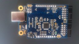
Yesterday I get the AK4490 boards. There is a delay with control boards, but they will be ready soon.
Now is the hard part - I have to write the firmware of the processor, which controls the AK4490 DAC. The AK4490 DAC has a plenty of options and I'll try to get them all 🙂 which can take a while.
Regards,
Joro
Attachments
- Home
- Source & Line
- Digital Line Level
- XMOS DSD 384 kHz / 32bit USB