If the CS was controlled in certain way,different loading could be handled by a parallel resistor off the main output board. I have always assumed the if you were able to see 10 N channel fets on one channel of his amp, that they were all of the same nature, but if he has a current source on each rail, then it impossible that they are just lined up that way for proper heat dissipation and thermal consistency and just maintained/driven in different ways. Perhaps the XA.8 only has 3 driver fets and 2 CS fets. Automatic higher bias per get by default. I love guessing wrong
I suspect that there are 4 IRFP240 and 5 IRFP9240 driver fets with 1 IRFP240 CS fet.
I am about to do a simple experiment using an F4. I will connect a bench supply operating as a CCS at +30V to output of one channel. Then, varying the CCS current, and rebalancing the F4 bias to maintain the proper values for the PFETs (IRFP9240) and adjusting the F4 offset to near zero volts, I will measure the harmonics.
This is a very simple experiment to test the approach and involved no circuit modifications to the F4. The same experiment could be applied to an F5. For some output stages, a negative CCS might be needed.
This is a very simple experiment to test the approach and involved no circuit modifications to the F4. The same experiment could be applied to an F5. For some output stages, a negative CCS might be needed.
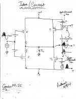
Idea for a combo PP-SE amp.
I understand that the technical objective is to operate a power output stage in a combination of Push Pull and Single Ended modes simultaneously. The image shows a possible method to do it.
1.The N an P devices [left of image] are complementary MOSFETs which are the power output stage.
2. These N and P devices are forward biased and are symmetrically driven by the half shaded input sinewave signal. This stage operates in Push Pull mode.
3. The complementary MOSFETs N1 and P1 are characterized as "dynamic current sources". Each device is separately forward biased [light or heavy].
4. A positive going analog pulse [1/2 wave rectified] is derived from the input [or output] signal. and then is superimposed on the forward bias voltage of device N1, such that its EMF adds to it.
5. In operation as the voltage of the input signal rises [shaded; above ground], device N1 is enabled to simultaneously conduct such that the operation of N and N1 is characterized as Single ended; meaning N1 is the dynamic current source to N; while the N and P devices do their push pull operation.
6. During the time interval of the shaded part of the sine signal [0 to t1 seconds], device P1 sat idle; totally unaware of the activity of the other 3 devices; especially N1.
7. Device N1 goes dormant at the end of time t1 of its positive pulse, and then P1 is awakened into deeper conduction by a negative going pulse [at time t1] which is time-coincident [[in phase] with that of the input or output sine wave [not shaded]. The devices N and P continue to operate push pull, and the devices P and P1 concurrently operate in SE mode with P1 acting as a dynamic current source to device P.
The most important point for this mode of combo PP-SE operation is that the pulses which are presented to the N1 and P1 devices are phase aligned with their counterparts in the parent input or the power output signals, and they [aka analog pulses] are [naturally] sequential in the time domain; but are not on top of each other or time coincident.
Attachments
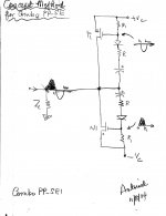
Idea for possible method to enable Combo PP-SE amp
The image shows that the power output node drives two independent half wave rectifiers which generate the requisite analog pulses at the gates of the N1 and P1 devices. These pulses sequentially drive N1 and P1 dynamic current sources so as to enable SE operation in the corresponding N and P devices of the power output stage which independently operate it push-pull.
The image shows that the power output node drives two independent half wave rectifiers which generate the requisite analog pulses at the gates of the N1 and P1 devices. These pulses sequentially drive N1 and P1 dynamic current sources so as to enable SE operation in the corresponding N and P devices of the power output stage which independently operate it push-pull.
Attachments
There's a dozen ways to skew the harmonic ratios in a push-pull Class A output stage, so pick one or a few and see what you get.
Keep in mind that it's not a magic bullet. I have of examples of circuits that sound better than others while still showing similar harmonic content.
And of course it's also a matter of personal taste, associated equipment, power levels and so on.
😎
Keep in mind that it's not a magic bullet. I have of examples of circuits that sound better than others while still showing similar harmonic content.
And of course it's also a matter of personal taste, associated equipment, power levels and so on.
😎
There's a dozen ways to skew the harmonic ratios in a push-pull Class A output stage, so pick one or a few and see what you get.
Keep in mind that it's not a magic bullet. I have of examples of circuits that sound better than others while still showing similar harmonic content.
And of course it's also a matter of personal taste, associated equipment, power levels and so on.
😎
In order to control the harmonic content of the final output, do you believe that it is useful for each stage of the amplifier to have minimal or highly controllable distortion? It is possible for the gain stage to have high levels of H2 which can be cancelled by the output stage having H2 of the opposite phase, but the higher harmonics are probably not cancelled. Thus, if the input and gain stages can made to have extremely low distortion, then the final output stage can be relegated to tuning the harmonic content, particularly if it is not part of a global feedback loop.
Hello Mr. Pass. This thread like others stimulates my imagination to make reasonable connections and find possible solutions to its puzzles. Your amps which operate in Super Symmetry essentially wipe out their internally generated harmonic distortions. It follows from this fact that operating an amplifier in a deliberate asymmetric mode [like you've done with others] enables harmonic distortion to sprout and be nurtured so as to present a pleasing enjoyment of music.There's a dozen ways to skew the harmonic ratios in a push-pull Class A output stage, so pick one or a few and see what you get.
Keep in mind that it's not a magic bullet. I have of examples of circuits that sound better than others while still showing similar harmonic content.
And of course it's also a matter of personal taste, associated equipment, power levels and so on.
😎
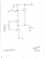
The attached image is a concept schematic of a PP power output stage onto which is superimposed a lopsided [asymmetric] mono lateral current source that bootstraps the N device. In my mind, this current source [constant or dynamic via switch ] operates with the bottom P device simultaneously in SE mode.
My hypothetical approach begs this question for an even simpler approach/solution to this asymmetric operation which lhquam had implicitly proposed in the above posts. Why strive [the DIYer] to have the absolute best complementary symmetry characteristics of the N and P output push pull devices [aka highly matched] when one may simply mismatch [e.g. their trans conductance] and use them deliberately; clearly absent a loop negative feedback which will defeat this purpose? It follows that in certain amp designs, the inherent lack of symmetry in the characteristics of complementary devices [prevalent in their commercial production] suggests it be welcomed instead of shunned!
Best regards.
Attachments
It follows that in certain amp designs, the inherent lack of symmetry in the characteristics of complementary devices suggests it be welcomed instead of shunned!
Absolutely. The other way to think about it is that you are always going
to have asymmetry between the N and P type parts, but assuming that you
match the N's as a group and the P's as a separate group, you can achieve
cancellation of the 2nd harmonic.
If that's what you want.
I need to point out again that we are not generally out to deliberately create
more distortion, rather we want to have more control over the relative
values of the harmonics.
😎
It's seems so easy to talk about. Basdd on my limited experience, I cannot imagine the time it took to tweak it.
The artwork in the image is from lhquam from an earlier post. I added my input to share with y'all because I do not want to keep its ideas in my head, and frankly I may not know and/or understand or appreciate the value of its results. Best that I leave the following in your capable hands to assess.
The science of solving a problem begins by separating its elements. For example, chromatography separates the chemicals in a mixture [aka a can of worms] for the later identification of each contributor by other means.
Figure 1 shows that I input either a positive or a negative pulse instead of a sinewave to the joined gates of this output stage. Here, I separated a positive or a negative pulse from its parent sinusoidal wave; clearly hoping to gain insight from this unilateral operation from the shape, amplitude etc. of the output pulse in relation to that I input to amp.
Figure 2 shows that I input a positive or a negative pulse to the gates of the N devices while the forward biased gates to the P devices were grounded by comparison. Another experiment is to reverse the said scheme; meaning ground the gates of the N devices, and input a positive or a negative pulse to the gates of the P devices. Here, I separated the gates of the N and P devices with additional intentions to understand unilateral performance of the devices.
The use of input sine waves [lhquam], and also pulses per above in testing is expected to shed a brighter light so as to further understand the operation of this output stage. Thus, one acquires additional independent simultaneous "equations" to work with for a clearer answer.
Best regards.
Attachments

assuming that you match the N's as a group
and the P's as a separate group, you can achieve cancellation of the 2nd
harmonic.
Someone just pointed out the error of this statement - I meant to say that
with balanced output stages you can achieve the cancellation.
😎
In order to control the harmonic content of the final output, do you believe that it is useful for each stage of the amplifier to have minimal or highly controllable distortion? It is possible for the gain stage to have high levels of H2 which can be cancelled by the output stage having H2 of the opposite phase, but the higher harmonics are probably not cancelled. Thus, if the input and gain stages can made to have extremely low distortion, then the final output stage can be relegated to tuning the harmonic content, particularly if it is not part of a global feedback loop.
That's pretty correct. Also this depends on an output stage which naturally
gives low order distortion - 2nd and 3rd, with 2nd being very dominant,
at least at low power levels. Inevitably this seems to mean high bias
current.
😎
Is the Pass Labs XA.8 series "Super-Duper Symmetry"?
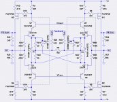
I have been seriously studying the 6Moons review of the Pass Labs XA.8 series amplifiers and the Pass Labs documentation. As stated in the 6Moons review, the XA.8 series draws upon the experimental designs of the FirstWatt products. The output stage is similar to the F4 or BA-2 hybridized with a single-ended CCS as in the BA-1. The front-end resembles the F5X and BA-3B but has the twist of cascoding and two additional adjustment pots in the input stage, and apparently no pots for adjusting the JFET drain loads.
I might have figured out the XA30.8 front-end based on the Pass Labs documents and the 6Moons Review. This schematic combined with my best guess about the output stage simulates very well, apparently meeting most or all of the performance specs. It required numerous design iterations of the interconnect topology of the JFET source pins and the feedback network before I found one that did the "right thing". I finally arrived at a hybrid of "X" and "H" topologies with P1 and P2 pots connected as in the BA-3B, and P3 and P4 pots connecting in the "X". I have not encountered any discussions of this topology.
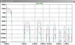
In LTSpice simulations, starting with all pots in the middle position, I adjusted P3 and P4 to set H2 and H3 to the same levels at 9 watts output. I then adjusted P1 and P2 to minimize the DC offsets of +/-FE-Out. A few iterations of the adjustments were required, resulting in the harmonic plots at 1W, 9W, 30W, and 60W output. Thus, the four pots adjust both H2 and the front-end output offset voltages.
The output stage bias appears to be closely related to that of the F4, with one additional resistor per phase which I suspect connect to thermistors on the heatsink next to the ribbon cable connector.
I am sure that there are still many mysteries to unravel about the XA.8. It would certainly be nice to hear one.
BTW: The simulations are with power supply rails of +/-25V.
I have been seriously studying the 6Moons review of the Pass Labs XA.8 series amplifiers and the Pass Labs documentation. As stated in the 6Moons review, the XA.8 series draws upon the experimental designs of the FirstWatt products. The output stage is similar to the F4 or BA-2 hybridized with a single-ended CCS as in the BA-1. The front-end resembles the F5X and BA-3B but has the twist of cascoding and two additional adjustment pots in the input stage, and apparently no pots for adjusting the JFET drain loads.
I might have figured out the XA30.8 front-end based on the Pass Labs documents and the 6Moons Review. This schematic combined with my best guess about the output stage simulates very well, apparently meeting most or all of the performance specs. It required numerous design iterations of the interconnect topology of the JFET source pins and the feedback network before I found one that did the "right thing". I finally arrived at a hybrid of "X" and "H" topologies with P1 and P2 pots connected as in the BA-3B, and P3 and P4 pots connecting in the "X". I have not encountered any discussions of this topology.
In LTSpice simulations, starting with all pots in the middle position, I adjusted P3 and P4 to set H2 and H3 to the same levels at 9 watts output. I then adjusted P1 and P2 to minimize the DC offsets of +/-FE-Out. A few iterations of the adjustments were required, resulting in the harmonic plots at 1W, 9W, 30W, and 60W output. Thus, the four pots adjust both H2 and the front-end output offset voltages.
The output stage bias appears to be closely related to that of the F4, with one additional resistor per phase which I suspect connect to thermistors on the heatsink next to the ribbon cable connector.
I am sure that there are still many mysteries to unravel about the XA.8. It would certainly be nice to hear one.
BTW: The simulations are with power supply rails of +/-25V.
Attachments
nice .
however , I didn't notice Papa's wink to proceed with that in public .....

........
I am sure that there are still many mysteries to unravel about the XA.8.....
however , I didn't notice Papa's wink to proceed with that in public .....
nice .
however , I didn't notice Papa's wink to proceed with that in public .....
You have a PM. 😉
P3/4 looks like a variation on what I saw in the Curl thread, except cross connected.I would think you would still need bias pots, but could be wrong. One rail could have fixed resistors an the other pots, like in past amps. Am I right in that p3/4 help adjust final harmonic structure between two halves of the channel.
P3/4 looks like a variation on what I saw in the Curl thread, except cross connected.I would think you would still need bias pots, but could be wrong. One rail could have fixed resistors an the other pots, like in past amps. Am I right in that p3/4 help adjust final harmonic structure between two halves of the channel.
My schematic is based on what was visible in the 6Moons pictures, the Pass Labs product descriptions, and previous publicly available designs by Nelson. The only pots visible on the input board are in the vicinity of the JFETs, rather than the cascode transistors, making it unlikely that any of the four pots are related with JFET drain loading.
Yes P3/P4 will affect the harmonic structure by changing the JFET load lines. Since all of the pots interact with one another in defining the harmonic structure, FE output gain and offsets, I am still struggling to understand exactly what is going on. There are 4 JFETs: ++, +-, -+, and -- which are +phase+rail, +phase-rail, -phase+rail, and-phase--rail resp. The P3 pot affects the gain of the ++ and -- JFETs, and the P4 pot affects the gain of the +- and -+ JFETs, and also cause to output offsets to change. It could be a tweakers nightmare.
During the development of diyF6 to now, I failed to grasp, and further appreciate the mechanism of action due to the so-called "pots" [e.g. P3 and P4 in post #94 above]. Is one deliberately tampering with the fidelity of the parent sine signal? By this I ask whether one strives to change the ratio of the area under the curve of the positive-going relative to the negative-going components of the sinusoid; which at the outset had both components identical [area, absolute amplitude]; or symmetric? Please elaborate. Thanks.
- Status
- Not open for further replies.
- Home
- Amplifiers
- Pass Labs
- XA.8 single-ended current sources