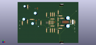
I am trying to connect components on a Mooly amplifier. I have chosen to make a mono board. I have absolutely now idea on what I am doing and do therefore think that I properly have made every mistake possible. I know I that what I have connected is connected in a random order, but do follow the rats-nest.
I did start by placing every component, acording to the schematic and then moved around as I thought looked somewhat okayish.
Please look at it and give some advice (after your chock!🙂
I did start by placing every component, acording to the schematic and then moved around as I thought looked somewhat okayish.
Please look at it and give some advice (after your chock!🙂
Attachments
I'll have a look later 🙂 but a couple of things I tend to do are to make traces and pads thick because when you see the real thing they will look very thin and fragile.
I also always tend to route boards manually by dragging parts around. Decide where the output devices will be on the board first as that will determine how everything else fits in around them. Yours looks like it could be essentially OK although I would look at making it more compact with parts closer together.
Have a look at post #22 here for an example of how I scale pads and traces:
GERMANIUM Single ended Class A Headphone Amp.
A basic way of doing it is use the rats nest but optimise the nets to get shortest routes.
I tend to line up all components near each other (i.e. lines of resistors)
Then perform a "swap autoplace" function which recursively swaps places of components that are the same to see if that improves net lengths. If it does it keeps new layout if not reverts back to how it was. This can shrink pcb by quite a bit and will keep tracks as short as possible.
+1, it is very un-optimal (non optimal?) an needs some work.The obvious observation is that the pcb is much larger than the circuit!
And don't forget to add holes to fix the board to the case.
Yes, the reason for the giant board and the missin holes is that I started by aranging the component as on the schematic and thought that, after aranging everything, I know where to place holes and so on. 🙂
Am I wrong in thinking that the neutral wire from the transformer is connected at the same place as the speaker out? Do that not give some "cross talk" I mean residual noise when power is going trough the power wire? Or can I just ignore that and place the wires near each other?
Am I wrong in thinking that the neutral wire from the transformer is connected at the same place as the speaker out? Do that not give some "cross talk" I mean residual noise when power is going trough the power wire? Or can I just ignore that and place the wires near each other?
The centre point of the transformer is ground but you mustn't use that actual point for grounding... you must create a clean ground by taking a short spur off from the reservoir caps.
That clean ground can go to your PCB.
If the power supply is shared between the channels then the speaker return is best taken back to the clean ground at the power supply and not direct to the amplifier PCB.
Post 38 here:
3 stage LIN topology - NFB tappings?
And post #45:
3 stage LIN topology - NFB tappings?
The rats nest fooled me, I did look at how the rats nest strings were pointing and awoided crossing if I could. But when trying to put track on, it did got to be a rats nest on steroids!
So I have to start all over again, great way to learn! .-)
So I have to start all over again, great way to learn! .-)
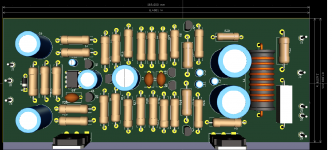
Your last picture looks very nice, the army is ready to engage.
But do follow Mooly's first or next law referenced in #2: Have tracks at appropiate width!
But do follow Mooly's first or next law referenced in #2: Have tracks at appropiate width!
Thanks, yes it was maybe nice looking, but the tracks would go across the whole PCB and back again, and on cross several plases. So it was just an error of design.
Hmm this is harder then expected, I do not understand KiCad's rats nest lines. Let's say I move a component and I place it, the lines change connection point to an other place, a place I do think the trace can go to. But when I have moved components to what I think can be okay, and the rats nest lines do show nearly no crossing and that all lines is fairly logical. And I then start using the track drawing tool, the track do in no way mach what the rats nest lines shows me. I can have two components that is shown to lie great, but with the track tool, do I suddenly have to go across the board, via 4 other components and finally back to the component I did put right beside the first component.
What am I doing wrong?
What am I doing wrong?
I use Diptrace but route the boards manually, and etch them manually as well using a UV lightbox 😱
I must get more up to date 🙂
I must get more up to date 🙂
Thanks for fixing my mistake🙂
I am also trying to rout manual, KiCad has no autorout function, but the rats nest is very confusing, when it points to something but show something else while routing.
Do you have a routed pcb in the Diptrace?
Do you think it could be usable for me?
I am also trying to rout manual, KiCad has no autorout function, but the rats nest is very confusing, when it points to something but show something else while routing.
Do you have a routed pcb in the Diptrace?
Do you think it could be usable for me?
I've nothing for this amp in Diptrace I'm afraid, I used pencil and paper when this one was made... that's even more old fashioned.
I've not studied KiCad but I thought it was supposed to be about the most comprehensive PCB package out there.... I actually have it and all the documentation installed.
It do say 🙂 to use Freerouter. Have you got all the documentation?
I've not studied KiCad but I thought it was supposed to be about the most comprehensive PCB package out there.... I actually have it and all the documentation installed.
It do say 🙂 to use Freerouter. Have you got all the documentation?
Attachments

Thanks a lot, not it does not look like I have all the documentation but I'll try to correct that🙂
Also have a look here:
FreeRouting | FreeRouting Documentation
All the KiCad pdf's are here:
Home | KiCad Docs
FreeRouting | FreeRouting Documentation
All the KiCad pdf's are here:
Home | KiCad Docs
Attachments

- Home
- Design & Build
- Construction Tips
- Worst PCB track-layout ever?