Nice.
What transistors suitable for an audio amplifier output stage have you found to have low enough di/dt to not create crossover distortion.
I'm curious because it would really be nice to get a low bias class AB output stage with no or little crossover distortion.
di/dt is decided by the signal and the load: for example a 1kHz 1A current crosses zero with a di/dt of 2pi A/ms. It's a measure of the rate of change of the current as it changes sign. So a higher di/dt at crossover means the transistor must turn off faster. But there is a limit to how fast it can turn off due to stored charge in the junction which is a property of BJTs. The stored charge has to be evacuated before it turns off, and if it stays on for too long when it should be off, then it will make a mess and you get a crossover spike.
When the driver applies a lower voltage to the base to turn the transistor off, the charge will be sucked out slowly via the base and it will also exit through the emitter. This takes a while, and the drivers are also driving the other transistor with the actual signal, so they can't "pull" the base of the transistor that is turning off more than what the actual signal says.
So there is a "figure of merit" for transistors, maybe we could call it "turnoff speed", which could be expressed as the highest di/dt where it still turns off smoothly. If it is asked to turn off faster than that, it begins to make spikes. This depends a lot on the transistor, and in my tests I did not see an obvious relationship with fT. I mean, lower fT transistors were worse, but between various "famous" transistors specified at similar fT there was quite a difference too.
I dug into my plots. Here's an example worst case, TIP41C-42C.
ok... this will probably be hard to read, the labels are on the plots so look for them... but I just want to point to the middle row of plots which is the base current. At each crossover you can see a bump, that's the drivers trying to pull charge from the base of the power devices. The two small plots on the right are a zoom on both crossovers. The legends are missing, but they're the same as the plot on the left, base current of both transistors (orange,blue) and total base current (green).
Now compare with one of the best cases, which is the famous MJL transistors, with higher bias, no emitter resistors, etc. During the crossover, base current is very smooth, there is no spike, the drivers don't fight it trying to turn it off:
The residual is also much smoother. Second graph on the bottom row is the FFT of the output voltage, you can compare the harmonic spread between the two (in blue), the difference is quite striking.
This is not just the transistors being better, it's also the fast drivers, and the lack of emitter resistors means the class-A region is much wider at the same bias, so this gives the transistor much more time to turn off. Basically it turns off at a lower di/dt, much lower than its maximum, so it is smooth.
Another important feature is shown in the last plot on the bottom right. X axis is the output current, and Y axis is the base current for both transistors. Due to capacitance creating phase shift between voltage and current, the IV curves on a XY plot "open" like a Lissajous curve, with more capacitance they look more like an ellipse. No capacitance would be a straight line. The slope is 1/hFe. Blue is top transistor, orange is bottom transistor, so if you see a bend ini the curve it means their hFe don't match. What's important to notice here is the MJLs have the same input capacitance whether they're on or off, and it is well matched between the two devices. But the TIPs do not, when one transistor is off, its capacitance disappears, and when it is on, it is much higher than the MJLs. So at crossover, there is a big change in hFe between the two transistors, and also a big change in input capacitance.
The SanKens 3519/1386 look similar to the MJLs, but they're a bit faster on fT, so you can get some extra open loop bandwidth for more feedback. That's the main difference. Otherwise they're both excellent devices.
One interesting thing was the OnSemi vs Toshiba A1942/C5200. The OnSemi's were much worse, more charge storage, and nonlinear hFe with current. Toshibas were much cleaner. Also cheap. Good choice if you need a lot of them.
Now if you want "low bias class AB output stage with no or little crossover distortion" that depends what you mean by "low". Because at low bias current, you still get the drop in gm at zero output current, so you still get static crossover distortion. Without emitter resistors, crossover distortion becomes very low at 100mA bias and it completely ceases to exist at 200mA bias, which is definitely not "low" but still not a class A space heater by any means.

Thanks for explaning...di/dt is decided by the signal and the load: for example a 1kHz 1A current crosses zero with a di/dt of 2pi A/ms. It's a measure of the rate of change of the current as it changes sign. So a higher di/dt at crossover means the transistor must turn off faster. But there is a limit to how fast it can turn off due to stored charge in the junction which is a property of BJTs. The stored charge has to be evacuated before it turns off, and if it stays on for too long when it should be off, then it will make a mess and you get a crossover spike.
When the driver applies a lower voltage to the base to turn the transistor off, the charge will be sucked out slowly via the base and it will also exit through the emitter. This takes a while, and the drivers are also driving the other transistor with the actual signal, so they can't "pull" the base of the transistor that is turning off more than what the actual signal says.
So there is a "figure of merit" for transistors, maybe we could call it "turnoff speed", which could be expressed as the highest di/dt where it still turns off smoothly. If it is asked to turn off faster than that, it begins to make spikes. This depends a lot on the transistor, and in my tests I did not see an obvious relationship with fT. I mean, lower fT transistors were worse, but between various "famous" transistors specified at similar fT there was quite a difference too.
I dug into my plots. Here's an example worst case, TIP41C-42C.
View attachment 1081705
ok... this will probably be hard to read, the labels are on the plots so look for them... but I just want to point to the middle row of plots which is the base current. At each crossover you can see a bump, that's the drivers trying to pull charge from the base of the power devices. The two small plots on the right are a zoom on both crossovers. The legends are missing, but they're the same as the plot on the left, base current of both transistors (orange,blue) and total base current (green).
Now compare with one of the best cases, which is the famous MJL transistors, with higher bias, no emitter resistors, etc. During the crossover, base current is very smooth, there is no spike, the drivers don't fight it trying to turn it off:
View attachment 1081706
The residual is also much smoother. Second graph on the bottom row is the FFT of the output voltage, you can compare the harmonic spread between the two (in blue), the difference is quite striking.
This is not just the transistors being better, it's also the fast drivers, and the lack of emitter resistors means the class-A region is much wider at the same bias, so this gives the transistor much more time to turn off. Basically it turns off at a lower di/dt, much lower than its maximum, so it is smooth.
Another important feature is shown in the last plot on the bottom right. X axis is the output current, and Y axis is the base current for both transistors. Due to capacitance creating phase shift between voltage and current, the IV curves on a XY plot "open" like a Lissajous curve, with more capacitance they look more like an ellipse. No capacitance would be a straight line. The slope is 1/hFe. Blue is top transistor, orange is bottom transistor, so if you see a bend ini the curve it means their hFe don't match. What's important to notice here is the MJLs have the same input capacitance whether they're on or off, and it is well matched between the two devices. But the TIPs do not, when one transistor is off, its capacitance disappears, and when it is on, it is much higher than the MJLs. So at crossover, there is a big change in hFe between the two transistors, and also a big change in input capacitance.
The SanKens 3519/1386 look similar to the MJLs, but they're a bit faster on fT, so you can get some extra open loop bandwidth for more feedback. That's the main difference. Otherwise they're both excellent devices.
One interesting thing was the OnSemi vs Toshiba A1942/C5200. The OnSemi's were much worse, more charge storage, and nonlinear hFe with current. Toshibas were much cleaner. Also cheap. Good choice if you need a lot of them.
Now if you want "low bias class AB output stage with no or little crossover distortion" that depends what you mean by "low". Because at low bias current, you still get the drop in gm at zero output current, so you still get static crossover distortion. Without emitter resistors, crossover distortion becomes very low at 100mA bias and it completely ceases to exist at 200mA bias, which is definitely not "low" but still not a class A space heater by any means.
Interesting...
I usually use as linear and good transistors as 2SA1942 and 2SC5200 but they still have around 0,05% crossover distortion on all harmonics when they turn off.
That's about how they perform without feedback.
That is not what I would say free from crossover distortion.
0,05% is very much audible for harmonics of the 7th order and higher.
So I assume there are no transistors better than that for output stages.
In my case anyway since I do not like or use global feedback when cross over distortion is present at the output stage.
I had some hope that you had found something very special and unique that basically have no or very little crossover distortion without using high bias class A.
You are most likely right.Or perhaps it's the layout, as he says "the layout was the limiting factor".
"By the form of the oscillograms of the residual signal for both transistors, the breadboard resonances dominate, the difference is small, and is determined mainly by the difference in the capacitances of the transistors. A really high-quality output stage should not have "ringing", especially for several periods, transients when switching arms , there should be just small bumps against the background of "smooth" non-linearity, noticeable only under maximum load."
Ah, no it is not possible. At least 100mA bias is necessary to mostly get rid of it.I had some hope that you had found something very special and unique that basically have no or very little crossover distortion without using high bias class A.
Now OP asked about "fastest transistors", it is necessary to look at the point where the transition frequency is lowest, so the amplifier can be made stable in the worst case. Usually this is at low Vce and high Ic.
Versus A1386
But SanKen measures at Vce=12V, they're cheating. It is too easy at 12V. We need the output to get much closer to the rail to not waste volts. 5V would be nice.
Last year I programmed it to step Vce and current and do network analyzer sweeps. Load is a resistor, there is an output inductor and a Zobel network in the output. 50R VNA output to drivers input.
Result: at Vce=5V, SanKen beats MJL.
The Russians don't appear to think it is a Russian part... And in any case even if it's a fake there doesn't appear to be anywhere to buy it.
https://vk.com/wall-133622382_136200?lang=en

https://vk.com/wall-133622382_136200?lang=en
It seems that rules aren't for everybody here...Some can do whatever they want.THE RULES
NOT ALLOWED:
Discussions of politics, ethnicity, religion, medical or other divisive issues of any sort.
That implies Russia has a thriving semiconductor industry, which is largely unknown to those in the West, like their superb audio systems.
We could ask the forum members from Russia to tell us more about these devices, as practically used in amplifiers.
We could ask the forum members from Russia to tell us more about these devices, as practically used in amplifiers.
Thanks for sharing your research data.Ah, no it is not possible. At least 100mA bias is necessary to mostly get rid of it.
Now OP asked about "fastest transistors", it is necessary to look at the point where the transition frequency is lowest, so the amplifier can be made stable in the worst case. Usually this is at low Vce and high Ic.
View attachment 1081747
Versus A1386
View attachment 1081748
But SanKen measures at Vce=12V, they're cheating. It is too easy at 12V. We need the output to get much closer to the rail to not waste volts. 5V would be nice.
Last year I programmed it to step Vce and current and do network analyzer sweeps. Load is a resistor, there is an output inductor and a Zobel network in the output. 50R VNA output to drivers input.
View attachment 1081753
View attachment 1081754
Result: at Vce=5V, SanKen beats MJL.
200mhz driver, 60mhz final, the fastest Szikai pair in the Universe 🙂Ah, no it is not possible. At least 100mA bias is necessary to mostly get rid of it.
Now OP asked about "fastest transistors",
Attachments
-
 Screenshot_20220817-060010_Word.jpg164.2 KB · Views: 231
 -
 Screenshot_20220817-060036_Word.jpg185.7 KB · Views: 229
 -
 Screenshot_20220817-060733_Word.jpg459.3 KB · Views: 219
 -
 Screenshot_20220817-061914_Word.jpg237.2 KB · Views: 206
 -
 Screenshot_20220817-063004_Samsung Internet.jpg226.8 KB · Views: 191
 -
 Screenshot_20220817-063103_Samsung Internet.jpg197.8 KB · Views: 212
Last edited:
Nice data, thank you. Is IO positive the NPN and IO negative the PNP?Ah, no it is not possible. At least 100mA bias is necessary to mostly get rid of it.
Now OP asked about "fastest transistors", it is necessary to look at the point where the transition frequency is lowest, so the amplifier can be made stable in the worst case. Usually this is at low Vce and high Ic.
View attachment 1081747
Versus A1386
View attachment 1081748
But SanKen measures at Vce=12V, they're cheating. It is too easy at 12V. We need the output to get much closer to the rail to not waste volts. 5V would be nice.
Last year I programmed it to step Vce and current and do network analyzer sweeps. Load is a resistor, there is an output inductor and a Zobel network in the output. 50R VNA output to drivers input.
View attachment 1081753
View attachment 1081754
Result: at Vce=5V, SanKen beats MJL.
The Russians don't appear to think it is a Russian part... And in any case even if it's a fake there doesn't appear to be anywhere to buy it.
https://vk.com/wall-133622382_136200?lang=en
Unfortunately that link only allows me to read a bit before being begged to register. Is the supposed manufacturer called LEFI? No hits on google for that being an actual company. Someone went to the trouble of making fake datasheets and fake physical parts? Pretty good mystery.
Just noticed that before translating, the original poster announcing the parts is "lefi" https://electronix.ru/forum/index.php?app=forums&module=forums&controller=topic&id=167670
Could be a trap, to mine your data.
Could be Chinese posing as Russians, which is going into mystery novel territory.
Take care, use anonymous mode in browser, if you really need to know more about those, I see no need, 5200 and 1943 pair are good enough for me.
Prices are not mentioned either.
Could be Chinese posing as Russians, which is going into mystery novel territory.
Take care, use anonymous mode in browser, if you really need to know more about those, I see no need, 5200 and 1943 pair are good enough for me.
Prices are not mentioned either.
EOL 🙁Search to 2SC6145/2SA2223 ( Digikey ) like a Dan D'Agostino !
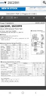
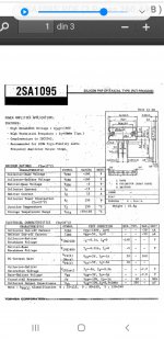
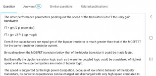
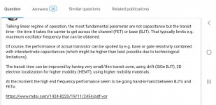
MOSFETs are faster. BJT is not particularly fast.
And the speed of the BJT is inversely proportional to the power.
And the speed of the BJT is inversely proportional to the power.
Really?! At what?MOSFETs are faster. BJT is not particularly fast.
You ca use Google for any question, trust me!
https://www.researchgate.net/post/Which_is_faster-BJT_or_MOSFET_and_why
Attachments


Last edited:
Yes, if I remember correctly.Nice data, thank you. Is IO positive the NPN and IO negative the PNP?
- Home
- Amplifiers
- Solid State
- Which is the fastest NPN/PNP pair power transistor for output stage?