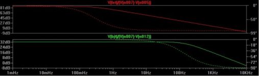
re: posts 694 and 695
Rodolfo, I don't understand what you have done with the gain char. of the bjt side. It is no longer operating as an op amp, as the open loop (OL) gain is ~32dB. Further, the open loop bandwidth (OLBW) is >10Hz, which means that the FFT setup jcx devised is not operating the bjts in the -6dB per octave/90 degree region.
I have attached two dual plots to show this discrepancy, one with your settings (Rodolfo fet_bjt_compare.jpg) and jcx's original setup as modified with added bjt emitter resistances of 210 ohms (jcx equal gain bjt_jfet.jpg).
The OL gain (dB) of the JFET side can be approximated by 20*log(R3/250), where 250 ohms is the FET dynamic resistance at 1mA. This works out as ~86dB, as noted in the plots.
The OL gain (dB) of the bjt side can be approximated by 20*log(R7/(210+re)), where re is about 26 ohms, the bjt dynamic resistance at 1mA. This also works out as ~86dB, as noted in the plots.
But, with your modified values, the OL gain on the bjt side drops to about 32dB, and the OLBW is >100Hz. It would appear that what you have done is to extend the OLBW to well above the bandpass where the bjt distortion products would fall. This would appear to give an entirely different picture than jcx's simulations.
Walt Jung
With this in mind, I modified both the Miller integrator resistor from 5 Megs to 10k and rised the feedback divider from the original 13 / 1 to 1300 /1. In doing so I lowered significantly the applied feedback.
The other variation is to include 210 ohm emitter resistors for the bjt pair - following jcx advise - bringuing the equivalent transconductance to aproximately the same as the one corresponding to the fet pair.
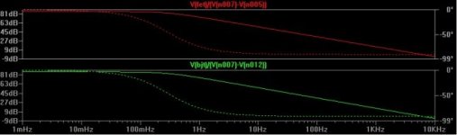
Rodolfo, I don't understand what you have done with the gain char. of the bjt side. It is no longer operating as an op amp, as the open loop (OL) gain is ~32dB. Further, the open loop bandwidth (OLBW) is >10Hz, which means that the FFT setup jcx devised is not operating the bjts in the -6dB per octave/90 degree region.
I have attached two dual plots to show this discrepancy, one with your settings (Rodolfo fet_bjt_compare.jpg) and jcx's original setup as modified with added bjt emitter resistances of 210 ohms (jcx equal gain bjt_jfet.jpg).
The OL gain (dB) of the JFET side can be approximated by 20*log(R3/250), where 250 ohms is the FET dynamic resistance at 1mA. This works out as ~86dB, as noted in the plots.
The OL gain (dB) of the bjt side can be approximated by 20*log(R7/(210+re)), where re is about 26 ohms, the bjt dynamic resistance at 1mA. This also works out as ~86dB, as noted in the plots.
But, with your modified values, the OL gain on the bjt side drops to about 32dB, and the OLBW is >100Hz. It would appear that what you have done is to extend the OLBW to well above the bandpass where the bjt distortion products would fall. This would appear to give an entirely different picture than jcx's simulations.
Walt Jung
Re: Unmatched Transistors...
Michael,
I understand that the excellent work by Ingrast is done on the simulator, which means that by definition the transistors of the same type are all matched, unless you deleberately UNmatch them by twiddling the modell parameters. So, unless this has been done, this is the situaltion with ideally matched transistors. Ingrast?
Jan Didden
Ultima Thule said:
JC,
so you say that unmatched transistors in the diffpair, or why not also the outputstage with 2 or more pairs, WILL add more distortion...
How dramatically is this?
However if we just focus on the input diff stage, I myself wondered this just for couple of days how an unmatched diffpair would distort compared to a matched pair.
I actually red Upupa Epop's comment in the issue seen in post #68 and #70 in another thread which got me thinking IF we use unmatched pair then each transistor will work under diffrent biasing condition and thereby parameters will be slightly offseted compared to each other.
But also, can DC servo fix the "problem"?
Michael
Michael,
I understand that the excellent work by Ingrast is done on the simulator, which means that by definition the transistors of the same type are all matched, unless you deleberately UNmatch them by twiddling the modell parameters. So, unless this has been done, this is the situaltion with ideally matched transistors. Ingrast?
Jan Didden
Re: Re: Unmatched Transistors...
Thanks for your comments, and indeed devices in the simulator are not just matched, but clones.
This brings a point of how much attention should be paid to this issue.
From the diyer perspective, the task of selecting devices for proper matching is viable though somewhat costly and time consuming.
From the comercial perspective, monolitic devices do match reasonably well, while discrete device matching probably is not economical. In this case it is my feeling techniques to work around the matching requirement are preferable.
Rodolfo
janneman said:
Michael,
I understand that the excellent work by Ingrast is done on the simulator, which means that by definition the transistors of the same type are all matched, unless you deleberately UNmatch them by twiddling the modell parameters. So, unless this has been done, this is the situaltion with ideally matched transistors. Ingrast?
Jan Didden
Thanks for your comments, and indeed devices in the simulator are not just matched, but clones.
This brings a point of how much attention should be paid to this issue.
From the diyer perspective, the task of selecting devices for proper matching is viable though somewhat costly and time consuming.
From the comercial perspective, monolitic devices do match reasonably well, while discrete device matching probably is not economical. In this case it is my feeling techniques to work around the matching requirement are preferable.
Rodolfo
Re: Re: Unmatched Transistors...
Janne,
thanks for your comments!
You confused my at first, I didn't have Ingrast's simulation work in my mind when wroting, the post was more IRL related.
I hope JC, or somebody else for that matter, will share with us some real life experience in the matter.
Upupa,
thanks for sharing your experience! 😎
I must admit, that JFET for input "sounds" nicer to me every day.
Regards
Michael
Re: re: posts 694 and 695
Hi Walt:
I scrambled back to the sim to find what I could have messed but couldn't. I must be overlooking something, for I do not find the discrepancy that should be bringing down the bjt gain down to 32 dB as you show.
Please advise which are the nodes (once you change something in the schematic, LTSpice will renumber them) you choose to compute the ploted responses (i.e. V(bjt)/(V(n007)-V(n012)) )
With respect to the OpAmp condition, I was not particularly concerned with keeping with the OL bandwith and rolloff. I interpreted the current subthread focused on input stage behavior, and in fact as I expressed previously, I somewhat dislike the idea of closing the loop with high gain ideal devices.
To that effect, the following post presents results where the loop is disposed off altoghether, so as to unveil the bare transfer characteristics of bjt vs. fet differential input pair.
Thank you for your comments Walt, will keep waiting.
Rodolfo
WaltJ said:
Rodolfo, I don't understand what you have done with the gain char. of the bjt side. It is no longer operating as an op amp, as the open loop (OL) gain is ~32dB. Further, the open loop bandwidth (OLBW) is >10Hz, which means that the FFT setup jcx devised is not operating the bjts in the -6dB per octave/90 degree region.
.......
Walt Jung
Hi Walt:
I scrambled back to the sim to find what I could have messed but couldn't. I must be overlooking something, for I do not find the discrepancy that should be bringing down the bjt gain down to 32 dB as you show.
Please advise which are the nodes (once you change something in the schematic, LTSpice will renumber them) you choose to compute the ploted responses (i.e. V(bjt)/(V(n007)-V(n012)) )
With respect to the OpAmp condition, I was not particularly concerned with keeping with the OL bandwith and rolloff. I interpreted the current subthread focused on input stage behavior, and in fact as I expressed previously, I somewhat dislike the idea of closing the loop with high gain ideal devices.
To that effect, the following post presents results where the loop is disposed off altoghether, so as to unveil the bare transfer characteristics of bjt vs. fet differential input pair.
Thank you for your comments Walt, will keep waiting.
Rodolfo
I'm attaching the file which produced my sims. You can simply run it. Nodes 007/012 are the inputs to the bjt stage, while V(bjt) is the output. Thus the labels on the plots are the mathematical expression for the op amp gain. You will see where the 32dB comes from simply by working the example you had used, i.e., R7=10k., emitter resistance = 210+26 ohms. It takes 5megs to get a bjt gain equal to the FET gain.
I don't understand your concerns about using the idealized SPICE devices, along with the real transistor models. This is a good concept, as it eliminates all sources of distortion, except that which is under study.
Walt
PS: rename the TXT extension to ASC to run the LTSpice simulation
Attachments
bare bjt - fet diff input pair
Delving further into the bipolar vs fet transistor technology for the differential input pair, I stripped the original test circuit by jcx of all loop feedback elements.
I kept the collector / drain current mirror loads and adjusted the bipolar pair emitter resistors to obtain the same voltage gain provided by the fet pair. This results in outrageous 39K values that only highlight the large difference in gain afforded by each. The large values nonetheless have the beneficial effect of greately improving stage linearity.
Biasing conditions are the same as previous tests.
Attachments

post 709
Rodolfo,
I don't know where you got the bjt 39k values from. They appear to be bogus.
As I said previously, to match the FET gain, the bjt total emitter R should be about 250 ohms. jcx matched this by making the external resistors 210 ohms, and with the internal bjt re of 26 ohms (for Ie=1mA), this is approximately met. My simulation shows that this is so. Yours should as well.
I suggest that you do an AC analysis, which shows these gain differences quite readily.
wj
Re: post 709
I agree with you, most certainly the bogus thing is the collector / drain loading with (almost) infinite resistance. I will run another test tomorrow with resistive loading, that will bring back gains to a predictable situation.
I am trying to upload the fft result but the gif exceeds the allowable size and have not at hand a suitable tool to correct.
Will nonetheless upload tomorrow the modified test circuit and results.
Rodolfo
WaltJ said:Rodolfo,
I don't know where you got the bjt 39k values from. They appear to be bogus.
As I said previously, to match the FET gain, the bjt total emitter R should be about 250 ohms. jcx matched this by making the external resistors 210 ohms, and with the internal bjt re of 26 ohms (for Ie=1mA), this is approximately met. My simulation shows that this is so. Yours should as well.
I suggest that you do an AC analysis, which shows these gain differences quite readily.
wj
I agree with you, most certainly the bogus thing is the collector / drain loading with (almost) infinite resistance. I will run another test tomorrow with resistive loading, that will bring back gains to a predictable situation.
I am trying to upload the fft result but the gif exceeds the allowable size and have not at hand a suitable tool to correct.
Will nonetheless upload tomorrow the modified test circuit and results.
Rodolfo
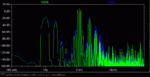
bare bjt - fet diff results
The previous test circuit yields the fft plot attached below.
This simulation is not a good approximation to reality as indicated in a previous post because of (almost) infinite impedance loading in the output devices. A better one is forthcoming.
The high level of harmonics and IM products are simply the result of bare device nonlinearities.
In this case, the result is more in line with what was to be expected in that the fet pair presents lower departures from linearity than the bjt pair even with gross emitter degeneration.
Yet, as could be seen in previous results, the higher gain afforded by the bjt pair can be used to advantage to correct and surpass performance, but then it should be noted the actual feedback elements should not degrade overall open loop response, that is, they should behave as nearly as possible to ideal devices as per simulation.
Rodolfo
Attachments
Rodolfo,
/philosophy mode on
Beyond the basic interesting question on the relative performance of the devices naked or otherwise, I find it intriguing that by degenerating the bjt we come very close to the fet. Yet they use very different physical properties. Or do they? There is some indication that there is a fundamental underlaying principle we haven't realised yet that governs BOTH devices, maybe even tubes.
You may think I have a couple of solder junctions corroded in my head (and the suggestion has been made before), but Mother Nature has a tendency to use a proven thing in just a slightly different way to come up with what looks like something very different, but really is a variation on a theme.
Maybe bjts and fets (and tubes) are variations on a common theme?
Wasn't it Douglas Hofstadler who studied creativity and concluded it really is "variations on a theme"?
/philosophy mode off
Jan Didden
The previous test circuit yields the fft plot attached below.
*What* previous test circuit?
wj
WaltJ said:
*What* previous test circuit?
wj
Post 709 Walt.
Attached is simulation file.
Please note this simulation is not good in the sense the only collector / drain load impedance is the own device's output one.
Rodolfo
Attachments
Re: re: post 715
Walt,
What was the Re for the bjt in these plots?
Jan Didden
WaltJ said:Here is an AC sim that shows matched bjt and FET gains.
Walt Jung
Walt,
What was the Re for the bjt in these plots?
Jan Didden
PMA said:According to the law of semiconductor physics 😉
OK, OK, no need to rub it in!😱
Jan Didden
- Status
- Not open for further replies.
- Home
- Amplifiers
- Solid State
- "What's your reasoning?" and not "What's your belief?".