fet - bjt input diff compare
Last post 716 regarding the comparison between a bjt and a fet input differential by Walt included a simulation of the bare open loop stage I made previously but including collector / drain resistive loading as I was planning to do.
Walt selected 250 ohms load I guess to establish a 0 dB voltage gain. Since the usual VAS that loads the input differential tends to present a higher impedance (and frequency dependent) I wanted to make a brief exploration with different resistive loadings and see the effects.
Another parameter to be considered is the bias point, so I also wanted to explore different biasing conditions but keeping constant voltage gain.
The simulation results - which I encourage others to review, critique and check for accuracy - reveal the situation benefits from a higher load impedance and is not very sensitive to bias operating point.
To limit output variables to a manageable quantity, I selected for measurement the first IM product at 12 Hz, and the second and third harmonics of the 10Hz component, though other choices are possible.
As an overall conclusion and only for the particular selected devices compared, it might be said a better than 80 dB performance for any individual spurious component may be achieved open loop with proper loading. The bipolar pair with emitter degeneration has a slight advantage particularly in the suppresion of second harmonic products.
Rodolfo
Attachments
open loop distortion comparison of bjt and fet
The quote above is what I thought I could do, but the system won't let me upload a 300k ZIP file.
wj
I am uploading a ZIP file which contains the source file (ASC) and the results (PDF) of a bjt and jfet for distortion, using LTSpice. It was found after much work that doing this open loop is much more sensitive to detecting the distortion of the two devices.
As will be noted, the schematic is very simple. The active devices are loaded with a resistance that yields a nominal gain of unity from V(Vin) to V(bjt) or V(fet). The FFT is done on the voltage across the load resistance, which is of course proportional to the current in the devices.
The driving waveform for the FFT is included in the PDF file and as can be noted, the level is quite low, i.e., 40mVp-p. See 100*V(vin)
For this test the bjt is not degenerated. In the results, the distortion is appreciably higher than that of the fet device. See 100*V(bjt) vs. 100*V(fet). Scaling is used to display a complete dynamic range.
Walt Jung
The quote above is what I thought I could do, but the system won't let me upload a 300k ZIP file.
wj
size of uploads
Walt:
I guess the size of the PDF's is giving you trouble.
Saving as GIF for images reduces considerably though the site will not allow you to upload images more than a certain width I do not remember just now, nonwithstanding file size.
A work around this last issue is to zip them or add a bogus suffix (e.g. .txt) to fool the server script though warning readers it is indeed an image.
Rodolfo
WaltJ said:
The quote above is what I thought I could do, but the system won't let me upload a 300k ZIP file.
wj
Walt:
I guess the size of the PDF's is giving you trouble.
Saving as GIF for images reduces considerably though the site will not allow you to upload images more than a certain width I do not remember just now, nonwithstanding file size.
A work around this last issue is to zip them or add a bogus suffix (e.g. .txt) to fool the server script though warning readers it is indeed an image.
Rodolfo
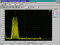
PMA said:And here is how it looks at the power amp output, the one that measures pretty good on single-tone analysis.
PMA:
I understand these are actual measurements with your high quality measurement gear?
Another proof complex well designed test signals are a must to exercise a device as the people from Audio Precision discuss.
Rodolfo
ingrast said:
PMA:
I understand these are actual measurements with your high quality measurement gear?
Another proof complex well designed test signals are a must to exercise a device as the people from Audio Precision discuss.
Rodolfo
Yes, they are the real measurements with FM modulated signal:
carrier = 10kHz
frequency deviation = 2kHz
modulating frequency = 200Hz
The result was shown for "class A 20W" amplifier. The best result obtained is for the "error correction amplifier" and I am attaching it now.
Attachments
Reprise of previous post #742
I am uploading a ZIP file which contains the source file (ASC) and the results (*.JPG) of a bjt and jfet for distortion, using LTSpice. This program is absolutely necessary to be able to view the schematic, but the JPG files may be viewed with any graphics program. It was found after much work that doing this comparison via open loop operation is much more sensitive to detecting the distortion of the two devices.
As will be noted, the schematic is simple. The active devices are loaded with a resistance that yields a nominal gain of unity measured from V(Vin) to V(bjt) or V(fet). The FFT is done on the voltage across the load resistance, which is of course proportional to the signal current in the devices.
The driving waveform for the FFT can be regenerated simply by running the transient simulation. As can be noted, the operating level is quite low, i.e., 40mVp-p. The FFT resulting from this is "fet_bjt_compare_openloop_Vvin.jpg".
For this test the bjt devices are not degenerated. The FFT resulting from the bjt test is "fet_bjt_compare_openloop_Vbjt.jpg".
The FFT resulting from the fet test is "fet_bjt_compare_openloop_Vfet.jpg".
In the results, the bjt distortion is appreciably higher than that of the fet device. See 100*V(bjt) vs. 100*V(fet). Scaling is used to display a complete dynamic range.
Walt Jung
11/09/2004
Attachments
fet_bjt_compare_openloop_b
fet_bjt_compare_openloop_b
A bjt/fet distortion comparison with
RE added such that VRE/Vt ~8
This ZIP file contains the source file (ASC) and the results (*.JPG) of a bjt and jfet for distortion, using LTSpice. This program is absolutely necessary to be able to view the schematic, but the JPG files may be viewed with any graphics program. This simulation file is adapted from fet_bjt_compare_openloop.ZIP, posted earlier on this date.
As will be noted, the schematic is simple. The active devices are loaded with a resistance that yields a nominal gain of unity measured from V(Vin) to V(bjt) or V(fet). The FFT is done on the voltage across the load resistance, which is of course proportional to the signal current in the devices.
The driving waveform for the FFT can be regenerated simply by running the transient simulation. As can be noted, the operating level is quite low, i.e., 40mVp-p. The FFT resulting from this is "fet_bjt_compare_openloop_Vvin_b.jpg".
For this test the bjt devices are degenerated, with added resistances of 210 ohms. The DC drop across these resistors is about 8 times that of Vt (Vt~0.026), or 0.210V.
The FFT resulting from the bjt test is "fet_bjt_compare_openloop_Vbjt_b.jpg".
The FFT resulting from the fet test is "fet_bjt_compare_openloop_Vfet_b.jpg".
In the results, the bjt distortion is now appreciably lower than that of the fet device. See 100*V(bjt) vs. 100*V(fet). Scaling is used to display a complete dynamic range.
Walt Jung
11/09/2004
Attachments
fet_bjt_compare_openloop_c
fet_bjt_compare_openloop_c
A bjt/fet distortion comparison with
RE added such that VRE/Vt ~38
This ZIP file contains the source file (ASC) and the results (*.JPG) of a bjt and jfet for distortion, using LTSpice. This program is absolutely necessary to be able to view the schematic, but the JPG files may be viewed with any graphics program. This simulation file is adapted from fet_bjt_compare_openloop.ZIP and fet_bjt_compare_openloop_b.ZIP, both posted earlier on this date.
As will be noted, the schematic is simple. The active devices are loaded with a resistance that yields a nominal gain of unity measured from V(Vin) to V(bjt) or V(fet). The FFT is done on the voltage across the load resistance, which is of course proportional to the signal current in the devices.
The driving waveform for the FFT can be regenerated simply by running the transient simulation. As can be noted, the operating level is quite low, i.e., 40mVp-p. The FFT resulting from this is "fet_bjt_compare_openloop_Vvin_c.jpg".
For this test the bjt devices are heavily degenerated, with added resistances of 1k ohms. The DC drop across these resistors is about 38 times that of Vt (Vt~0.026), or 1V. The load resistance is adjusted so that the nominal stage gain is still unity, and within 0.1dB of the comparison fet stage.
The FFT resulting from the bjt test is "fet_bjt_compare_openloop_Vbjt_c.jpg".
The FFT resulting from the fet test is "fet_bjt_compare_openloop_Vfet_c.jpg".
In the results, the bjt distortion is now appreciably lower than that of the fet device, and is also lower than the comparable bjt test within fet_bjt_compare_openloop_b.ZIP. See 100*V(bjt) vs. 100*V(fet). Scaling is used to display a complete dynamic range.
Walt Jung
11/09/2004
Attachments
Nonlinear correction
Spawned by a mention by Janneman several posts back, I quoted my personal expectations regarding adaptative nonlinear correction technologies for effectively compensating in this particular case an audio amplifier transfer.
I said then static transfer correction methods are limited by the fact they take into account only s-plane origins and immediate neighborhood, and that a complex nonlinear C(s) correction is needed in the general case.
Well, it now dawned on me the "s-plane origins and neighborhood" is - as everything else - something relative. To be more precise, if the amplifier to be corrected has essentially frequency independent behaviour within the audio band of interest, and withing the magnitude of perturbations to compensate, then a static correction should in principle work.
It will not be capable of self-adaptation to component tolerances, aging and environmental variations, but could probably be a good step forward.
If there is interest in this issue, then may be we could start an independent thread to exchange ideas and experiences in this respect.
Rodolfo
Rodolfo,
I would be interested, I could - possibly as a start - contribute my effort to make the feedback path Aol dependent. Not sure where it will get us though.
Jan Didden
I would be interested, I could - possibly as a start - contribute my effort to make the feedback path Aol dependent. Not sure where it will get us though.
Jan Didden
Walt,
Interesting results. You didn't mention it specifically, but I gather that in all cases the bias current was 1mA per device?
I have a question:
- There is some intermediate stage where the bjt and the fet distort equally (near 200 Ohms bjt degeneration?). Not being able to display your schematic, what were the two load resistors? I mean, which of the two had the gain advantage in that equal distortion point?
Jan Didden
Jan,Walt,
Interesting results. You didn't mention it specifically, but I gather that in all cases the bias current was 1mA per device?
I have a question:
- There is some intermediate stage where the bjt and the fet distort equally (near 200 Ohms bjt degeneration?). Not being able to display your schematic, what were the two load resistors? I mean, which of the two had the gain advantage in that equal distortion point?
Jan Didden
On question one, yes, the operating current is in all cases 1mA/side for both diff. pairs. You should get LTSpice, then you could see it all, and run your own sims.
On q2, there is only one load resistor, which loads the current mirror. This will be more obvious if/when you see the program. I really tried to sidestep this issue, but uploading the schematic file... but that's when I ran into the file size limits of this forum. Ugh! 🙁
The 210 ohm bjt RE value is likely very close to where the fet and bjt are near-equal in total distortion, but I didn't try to explore the exact point. But note also that this doesn't say anything about the order of the harmonics.
For LTSpice, see: http://www.linear.com/designtools/softwareRegistration.jsp
Walt Jung
OK Mr Curl.....i reckon even you will now concede that NO evidence has been produced to substantiate the myth that global negative feedback is a 'bad thing', to be used sparingly, or preferably, not at all....
On the contrary, you and its detractors can now be satisfied by the heaps of evidence proving that GNF reduces all known distortion, provided a sufficient quantity is employed... 😎
On the contrary, you and its detractors can now be satisfied by the heaps of evidence proving that GNF reduces all known distortion, provided a sufficient quantity is employed... 😎
Oh, crap......he's back!
Gee, Mikey, it was nice and quiet with you away. However did we pass the time without your cheery and pleasant presence?
(It is just a joke......don't blow gasket.)
Why not regale us with stories of your trip to the AES convention instead.
Jocko
Gee, Mikey, it was nice and quiet with you away. However did we pass the time without your cheery and pleasant presence?
(It is just a joke......don't blow gasket.)
Why not regale us with stories of your trip to the AES convention instead.
Jocko
Mikeks, I don't know if you are English or not, but you are an embarrasment to the rest of us if you are.
Shutup, go take a chill pill and stop winding everyone up - most of us are in this for the fun of it - not to prove how brilliant we are (which clearly you are).
Long live JC, NP, JB etc (and RIP JLH)
Shutup, go take a chill pill and stop winding everyone up - most of us are in this for the fun of it - not to prove how brilliant we are (which clearly you are).
Long live JC, NP, JB etc (and RIP JLH)
ACR said:Mikeks, I don't know if you are English or not, but you are an embarrasment to the rest of us if you are.
Shutup, go take a chill pill and stop winding everyone up - most of us are in this for the fun of it - not to prove how brilliant we are (which clearly you are).
Long live JC, NP, JB etc (and RIP JLH)
Drew,
Maybe you should just look through his tone, he HAS a point, even if he makes it quite awkwardly😉
BTW, who is JB?
Jan Didden
BTW, who is JB?
James Bond, aka 007, longform 0.007% THD excellent excellent sound without GNF.
It has been my experience that negative feedback is something that I prefer to minimize and eliminate, if possible. There is another type of distortion that might be important, that has not been discussed. This distortion was found by Dr. Hirata and uses a special test box to evaluate. Perhaps we should analyze this distortion mechanism as well. Hirata's papers can be found in the 'Journal of the AES' around 1980. Perhaps someone can find or provide a link.
Sometimes stuff sounds better with feedback, sometimes it
doesn't. If you have a decent set of ears, they will tell you.
😎
doesn't. If you have a decent set of ears, they will tell you.
😎
- Status
- Not open for further replies.
- Home
- Amplifiers
- Solid State
- "What's your reasoning?" and not "What's your belief?".