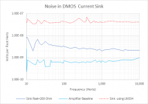
LM334 current is a function of temperature (227uV/C) and it's noise is likely higher than a resistor. See the datasheet.
Just measured the noise of the DMOS sink using a single resistor to set the current @ 10mA and an LM334 for 10mA. The measurement amplifier is one of Gerhard's designs and baseline noise is shown.
One other thing to note is temperature drift also initiated by self-heating of the LM334, but noise is more problematic.
Attachments
Last edited:
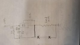
I think my problem is related to how the gate is connected in the circuit.
With the gate tied to the high side of the load, the zener provides a current path around the LM334.
If I tie it to ground, then the zeners provide a low impedance path to ground around the load. It "works" when simulated, but even if they are in series with the gate stopper to ground, there is still a high amount of current flowing through this path, much greater than what my supply is capable of providing.
Any resistance high enough in series with the zeners to limit their current to a manageable amount just ends up dropping a lot of voltage across said resistors and leads to a high Vgs.
Just really stumped on a solution right now.
You don't need normally a protection diode , you did the circuit wrong that's why the Mosfet blew ... Tho separate issues .
Of course you can add a protection diode , something like 15V that will allways be higher than the LM334 voltage
Last edited:
You don't have an LR8 to try, do you?
Noise as a current sink -- can do that soon.
The analysis of the LM334 motivated by WJ's response to a reader's correspondence with respect to the use of LM317 as a current source -- it's noisy.
The gate of the Mosfet should be tied to V- of the regulator , not ground .
In the link the schematic is correct , but that is for sinking current so the load is on the other side between + and the drain of the Mosfet
If you want to generate current you put the load from V- and Gate to ground .
This CCS doesn't need ( if I'm correct ) a permanent connexion to ground , it is self biasing or how is called .
You don't need normally a protection diode , you did the circuit wrong that's why the Mosfet blew ... Tho separate issues .
Of course you can add a protection diode , something like 15V that will allways be higher than the LM334 voltage
I'm a bit confused by these replies reading them again.
I've always had the load connected to V- of the 334. I substituted a 1k resistor for the tube after the first FET went just to eliminate that variable, but I've never configured it as a current sink. It is going to be an active load.
What is puzzling me is this:
https://audioxpress.com/assets/upload/files/Sources_101_P1.pdf
Ref diagram 7a, cascode configuration.
The gate of the JFET is tied to V- and the high side of the load. That's how I had things configured originally, with and without a gate stopper.
If I have the gate tied to ground, the gate will be at 0v. If the load is connected to the V- of the LM334, there will be ~249v present at the drain, correct?
If my Vgs (max) is +/-20v, how is any FET going to survive at high voltage supply?
When I put it on the breadboard and keep the supply voltage below 18v, it works with the gate grounded. But in that configuration, I'm within Vgs(max). I haven't applied HV to it because I'm pretty sure I know what is going to happen...and I only have one FET left until UPS shows up tomorrow.
As I stated, I'm only doing this to have a consistent current reference. I've gotten a DN2540 cascode to work, along with a PNP cascode. The PNP cascode actually performed the best in terms of gain, but I get some odd distortion/ringing on the sine wave just before the wave reaches its peak - voltage. I suspect it probably has something to do with my selection of transistors, so I've got a variety of others on the way to try.
I tried to explain that this CCS is like a 2 terminal component , the load to plus+ for sink and load to ground for source - as you want for your project .
If the gate is connected to ground like in your diagram the Mosfet will blow as soon as the voltage on the load ( tube ) will rise above 20V , max Vgs . That's why can't be correct like that .
If the gate is connected to ground like in your diagram the Mosfet will blow as soon as the voltage on the load ( tube ) will rise above 20V , max Vgs . That's why can't be correct like that .
Attachments
Last edited:
the fragile oxide layer will be ruptured with even a momentary voltage of 20V or more across gate-source.
I designed a class ab amp with same fet front end.
I applied a sine wave to the input to the amp.
I ramped it right up to see how loud it would go and it suddenly stopped working. When I looked at output of sig gen it was over 20 volts and thats what blew it. A change of fet and the amp was fine.
I tried to explain that this CCS is like a 2 terminal component , the load to plus+ for sink and load to ground for source - as you want for your project .
If the gate is connected to ground like in your diagram the Mosfet will blow as soon as the voltage on the load ( tube ) will rise above 20V , max Vgs . That's why can't be correct like that .
Ok, we're on the same page then. Thanks.
I wonder if that mosfet would blow up. My reasoning is for the mosfet to conduct any curent the gate has to have a voltage of 3 to 5 v higher than the source. And if the gate is grounded it defently isn't at 5v above the source.
I wonder if that mosfet would blow up. My reasoning is for the mosfet to conduct any curent the gate has to have a voltage of 3 to 5 v higher than the source. And if the gate is grounded it defently isn't at 5v above the source.
DN2540 is a depletion mode MOSFET, so it is fully on when the gate is at 0 Vgs
Last edited:
I was refering to the circuit in post 46.
Yeah, that's mine. I used the wrong symbol.
How long have you lived in Tyrone? I lived over at Canongate when I was in HS in the early-mid 90s.
Why are you folk bent on gilding a t*rd -- the design shown on DIYTUBE is both noisy and temperature dependent. Should be relegated to the trashbin of bad DIY designs.
I moved to Tyrone back in 1986 back then when you asked someone there phone # all they gave you was the final 4 digits.
Why are you folk bent on gilding a t*rd -- the design shown on DIYTUBE is both noisy and temperature dependent. Should be relegated to the trashbin of bad DIY designs.
That site shows up in my searches a lot and I agree the designs aren’t good.
Why are you folk bent on gilding a t*rd -- the design shown on DIYTUBE is both noisy and temperature dependent. Should be relegated to the trashbin of bad DIY designs.
That site shows up in my searches a lot and I agree the designs aren’t good.
I moved to Tyrone back in 1986 back then when you asked someone there phone # all they gave you was the final 4 digits.
I remember doing that too. It was only when I needed to call someone in Newnan did I have to ask for the rest of the phone number.
Why are you folk bent on gilding a t*rd -- the design shown on DIYTUBE is both noisy and temperature dependent. Should be relegated to the trashbin of bad DIY designs.
At this point, I just want to make the damn thing work out of frustration now.
I liked the simplicity of it, 4 components and biases itself. I’m all ears for suggestions on a less than 10mA design that isn’t too dependent on variations between components.
I'm curios how stable this CCS is with temperature , as we know LM334 is temperature dependent and could be used as temp sensor ...
Why are you folk bent on gilding a t*rd -- the design shown on DIYTUBE is both noisy and temperature dependent. Should be relegated to the trashbin of bad DIY designs.
It would be helpful if you provide an alternative design that works better, according to your criteria.
Last edited:
- Home
- Amplifiers
- Tubes / Valves
- What is killing my MOSFET (Tube CCS)