> How likely is it that components get damaged but don't completely die so the end product still suffers.
Applying more than -5 or -6V of Vbe (reverse bias) to almost any bipolar transistor will often leave a device still working, but with degraded Hfe and noise.
Applying more than -5 or -6V of Vbe (reverse bias) to almost any bipolar transistor will often leave a device still working, but with degraded Hfe and noise.
Talking about the dn2540 most talk centers on using this device at low currents would it still give good performance as a 100 ma plate load for a 6as7 .
You’d probably need to use the TO-220 version to make sure you don’t exceed the PD on the device, but no reason why it shouldn’t work.
Yes I was planing on using the TO-220 part as i will be disipating almost 5 watts so it will require a good heatsink or I may use it as the lower device in a ccs cascode with the upper device disipatimg most of the power.
unfortunately this works the other way round, too
you can easily charge your body by walking over a carpet made of synthetic materials,; if you now pick up a mosfet part for soldering, this charge (up to 100pf charged to several kV) kills the mosfet gate *because* your iron is grounded ...
when I worked in the industry long time ago they exclusively used those Weller irons which had a safety transformer and 12V heaters with just 2 wires and deliberately no safety earth connection; instead all workers handling mosfet components in both lab and production had to wear wrist straps which were earthed through several series connected megohm resistors to prevent the person and the components being charged; you could get fired if you didn't wear your strap ...
Working ESD safe is probably indeed a field of lenghty discussions... Besides cleaning my soldering iron so the tip was at gnd level again (measured less than 2 ohms between tip and ground on the power plug), I used the wrist strap. My hope was that everything is than at ground level. The DNs that I soldered like this worked well.
Thanks for the reply!
erik
When I grounded my soldering iron I
> I assume that the effective load would be the output impedance of this stage in parallel with the the following one, then use ohms law to determine the noise voltage?
Yes, that will translate the data sheet spec into V/rt.Hz. You can extrapolate the typical values curves to suit the current you plan to run, and use them to take account of frequency.
Since you are nearly there with the build, do an early noise test! I would run the CCS into a single resistor, similar to the real load, and check the rms noise for real. Then you can calculate where it will get to at the speaker end, where S/N can be considered (e.g. at 1 Watt output, rms comparing rms noise).
I will do just that. I've got another 15 of them on the way and will pick this back up when I get my new order, hopefully tomorrow. Thanks again for all the help.
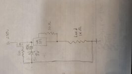
Ok, if someone could look this over before I start letting the smoke out of components again.
If I am not mistaken, I will need the 47k resistor to limit the current (5mA) through the Zener, otherwise it will be shorted to ground once the source voltage rises above Vz.
If I am not mistaken, I will need the 47k resistor to limit the current (5mA) through the Zener, otherwise it will be shorted to ground once the source voltage rises above Vz.
Attachments
I just don't think that is going to work. As I reed it you will have the gate of that mosfet tied directly to ground through the 100 ohm resistor. That will keep the mosfet off and no curent will flow through the rest of the circuite. Now i have been known to be wrong but I kind of think if you power it up it won't blow up it just won't do anything. But as I said I could be wrong.
I hope you didn't use that wrong schematic all the time ... the load shouldn't be connected inside but the CCS has 2 terminals and the load is from the minus side to ground .
Like this for sure the G-S max voltage would be exceeded easilly as the load + LM334 is in parallel .
Like this for sure the G-S max voltage would be exceeded easilly as the load + LM334 is in parallel .
Last edited:
I hope you didn't use that wrong schematic all the time ... the load shouldn't be connected inside but the CCS has 2 terminals and the load is from the minus side to ground .
Like this for sure the G-S max voltage would be exceeded easilly as the load + LM334 is in parallel .
The one from the link I provided or the schematic I’ve drawn?
I have the load connected to the V- terminal of the LM334.
My uncertainty involves where the gate should be connected. Rod stated I should add the Zener to protect the gate of the MOSFET, unless I misinterpreted how it should be connected.
The gate of the Mosfet should be tied to V- of the regulator , not ground .
In the link the schematic is correct , but that is for sinking current so the load is on the other side between + and the drain of the Mosfet
If you want to generate current you put the load from V- and Gate to ground .
This CCS doesn't need ( if I'm correct ) a permanent connexion to ground , it is self biasing or how is called .
Last edited:
The gate of the Mosfet should be tied to V- of the regulator , not ground .
In the link the schematic is correct , but that is for sinking current so the load is on the other side between + and the drain of the Mosfet
If you want to generate current you put the load from V- and Gate to ground .
This CCS doesn't need ( if I'm correct ) a permanent connexion to ground , it is self biasing or how is called .
Yes, it is an active load for the plate of a 6SN7, so my previous tests had the load connected to the V- terminal, and the gate is connected to ground through the gate stopper.
OK , now you know the problem 😀 , the good part is that is not a design error and could work if you do it right .
I never thought about the need for a grounded soldering iron. I wondered why mine had a 3 prong plug...
How likely is it that components get damaged but don't completely die so the end product still suffers.
After destroying some JFET opamps I realized I had ~40V on the tip of the iron. I now power the iron from a sine wave inverter off of a car battery...
I'm not sure if I'm over thinking something, or I still lack something in my understanding of the operation of the circuit.
If the gate is tied to ground (directly or through the stopper) it is now at 0v.
The source will be at the supply voltage of 250v minus the drop across the FET.
So my Vgs is -250. The zener as drawn, really isn't doing anything. I will just have 5v at the cathode of the zener. The source will still be at ~250v and the FET will die from exceeding Vgs(max).
If I connect the gate to the V- terminal of the LM334 (which is also where the high side of the load is connected) with the zener across the source and gate, the FET doesn't die, but the LM334 isn't doing anything. The current just changes with applied voltage. Makes sense because the zener+resistor are just in parallel with the LM334, and has a much lower impedance than the '334. Is there a way to provide gate protection with the zener that avoids this?
I'm about to the point of scrapping the whole thing and just dealing with having to manually trim a FET cascode with a pot, or just hand sort them for Vgs. Again, the point of using the LM334 was to eliminate the variability in Vgs between examples of the FET.
I tie the gate to the source with a bidirectional 12V TVS diode in my SE MOSFET source follower amp, but it's a depletion mode part. No more blown FETs. Not sure if that would work for you.
I tie the gate to the source with a bidirectional 12V TVS diode in my SE MOSFET source follower amp, but it's a depletion mode part. No more blown FETs. Not sure if that would work for you.
I think my problem is related to how the gate is connected in the circuit.
With the gate tied to the high side of the load, the zener provides a current path around the LM334.
If I tie it to ground, then the zeners provide a low impedance path to ground around the load. It "works" when simulated, but even if they are in series with the gate stopper to ground, there is still a high amount of current flowing through this path, much greater than what my supply is capable of providing.
Any resistance high enough in series with the zeners to limit their current to a manageable amount just ends up dropping a lot of voltage across said resistors and leads to a high Vgs.
Just really stumped on a solution right now.
Last edited:
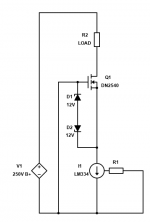
Usually it would look like the attached picture, where R2 is the load/circuit you want to pass the constant current through.
edit: ps. I quickly drew the circuit using an online schematic creator.
https://www.digikey.com/schemeit/project]Blocked
edit: ps. I quickly drew the circuit using an online schematic creator.
https://www.digikey.com/schemeit/project]Blocked
Attachments
FWIW, I tried that using back to back 12V zener diodes and my MOSFET still blew up. That's why I went with a TVS diode.
I used one of these... SA12CA - SA Series - Leaded TVS Diodes - Littelfuse
I used one of these... SA12CA - SA Series - Leaded TVS Diodes - Littelfuse
Have you tried using a 10M45S instead? They're a lot less finicky than the one you're using. The TO-220 version is pretty cheap and they are robust. Just use a 1k resistor on the gate and a 300r resistor at the source and that'll give you a clean 10ma CCS that works up to 450v or so.
- Home
- Amplifiers
- Tubes / Valves
- What is killing my MOSFET (Tube CCS)