The refrigerator is right around the corner too. 😉Do you still use a rotary dial telephone? 😀
Classic. I have one but I never use it. I haven't used a land line since the 90's other than the odd payphone...
Couldn´t care less about body weight, wind speed, bolt diameter or thread, etc. , because we are not talking about them here. I clearly stated "in PCB design" , period.
Please don´t use straw man arguments with me.
FWIW I hate fractional measurements, be them Imperial or not, or non Base 10 scales (hey, I even hate Binary and Hexadecimal too); I am a dyed in the wool Metric guy, but reality is that in the Component World Mil rules .... literally 😉
7.5 mm spacing Electrolytics are "acceptable" because of non critical lead spacing which anyway is clearly a multiple of an inch based scale, decimal of course which is my point, in this case 300 mils.
The slight error is well within tolerance and in any case you are dealing with two legs only.
Try that with any Op Amp, or most other ICs, transistors, etc.
Check:
https://en.wikipedia.org/wiki/List_of_integrated_circuit_packaging_types
Notice most (even if "mm dimensions are mentioned") give out round or simpler numbers under Imperial rule (again, I am speaking mils here, non 247/364ths of an inch or any similar nonsense) and weird "head breaking" are the ones in mm.
OR, wide enough tolerances are given to cover for the errors.
But back to the main point: here we are trying to help our friend hadmatter design his own PCBs.
Which to boot will be TUBE PCBs , and presumably use standard through hole components, where mils are the standard, no Arduino/DSP stuff here.
So I fully agree with experienced ruffrecords suggestion: "setup PCB design software to Imperial scale which there means "in mils"
The day he wants to design a cellphone, yes, he will probably be better served using Metric, why not? 😉
PS:even in non through hole stuff, mils apply, go figure.
As in:
Please don´t use straw man arguments with me.
FWIW I hate fractional measurements, be them Imperial or not, or non Base 10 scales (hey, I even hate Binary and Hexadecimal too); I am a dyed in the wool Metric guy, but reality is that in the Component World Mil rules .... literally 😉
7.5 mm spacing Electrolytics are "acceptable" because of non critical lead spacing which anyway is clearly a multiple of an inch based scale, decimal of course which is my point, in this case 300 mils.
The slight error is well within tolerance and in any case you are dealing with two legs only.
Try that with any Op Amp, or most other ICs, transistors, etc.
Check:
https://en.wikipedia.org/wiki/List_of_integrated_circuit_packaging_types
Notice most (even if "mm dimensions are mentioned") give out round or simpler numbers under Imperial rule (again, I am speaking mils here, non 247/364ths of an inch or any similar nonsense) and weird "head breaking" are the ones in mm.
OR, wide enough tolerances are given to cover for the errors.
| Acronym | Full name | Remark |
|---|---|---|
| SIP | Single in-line package | |
| DIP | Dual in-line package | 0.1 in (2.54 mm) pin spacing, rows 0.3 in (7.62 mm) or 0.6 in (15.24 mm) apart. |
| CDIP | Ceramic DIP[1] | |
| CERDIP | Glass-sealed ceramic DIP[1] | |
| QIP | Quadruple in-line package | Like DIP but with staggered (zig-zag) pins.[1] |
| SKDIP | Skinny DIP | Standard DIP with 0.1 in (2.54 mm) pin spacing, rows 0.3 in (7.62 mm) apart.[1] |
| SDIP | Shrink DIP | Non-standard DIP with smaller 0.07 in (1.78 mm) pin spacing.[1] |
| ZIP | Zig-zag in-line package | |
| MDIP | Molded DIP[2] | |
| PDIP | Plastic DIP[1] |
But back to the main point: here we are trying to help our friend hadmatter design his own PCBs.
Which to boot will be TUBE PCBs , and presumably use standard through hole components, where mils are the standard, no Arduino/DSP stuff here.
So I fully agree with experienced ruffrecords suggestion: "setup PCB design software to Imperial scale which there means "in mils"
The day he wants to design a cellphone, yes, he will probably be better served using Metric, why not? 😉
PS:even in non through hole stuff, mils apply, go figure.
As in:
JEDEC and JEITA/EIAJ standards
Small outline actually refers to IC packaging standards from at least two different organizations:
- JEDEC:
- JEITA (previously EIAJ, which term some vendors still use):
- Semiconductor Device Packages. (EIAJ Type II is 5.3 mm body width, and slightly thicker and longer than JEDEC MS-012.)
Note that because of this, SOIC is not specific enough of a term to describe parts which are interchangeable. Many electronic retailers will list parts in either package as SOIC whether they are referring to the JEDEC or JEITA/EIAJ standards. The wider JEITA/EIAJ packages are more common with higher pin count ICs, but there is no guarantee that an SOIC package with any number of pins will be either one or the other.
However, at least Texas Instruments[1] and Fairchild Semiconductor consistently refer to JEDEC 3.9 and 7.5 mm width parts as "SOIC" and to EIAJ Type II 5.3 mm width parts as "SOP".
Last edited:
I'm still trying to figure out why they call them "mils" instead of "thous"... When I was a kid, I thought "mils" were millionths of an inch.
In any case, I will continue to use Metric. You use mils, and the OP can use whatever they damned well please, right? It's a (mostly) free world 🙂
When I go to EasyEDA, the defaults are metric. Changing to mils gives a default board size of 3937.01 x 3937.01 mils which is a stupid way of saying 100mm x 100mm IMHO. Changing to inches is no longer an option, either.
About 1960, the US government announced that America would convert to metric.
. . . Some things take time.
. . . Some things take time.
Thou is the British term for one thousandth of an inch. For reasons best known to themselves, the Americans decided to call it mil.I'm still trying to figure out why they call them "mils" instead of "thous"... When I was a kid, I thought "mils" were millionths of an inch.
Cheers
Ian
mil = milli inchThou is the British term for one thousandth of an inch. For reasons best known to themselves, the Americans decided to call it mil.
Cheers
Ian
The inrush current into cold heaters does not depend on whether you turn them on "before power" - whatever you mean by this ...Ok, so sounds like everything should be pretty low current if I make sure to turn on the heater before power, but ...
Been there done that. Some of the cell phones I designed in the late 90's and early 2000's were done in inches, or fractions thereof. Things moved over to metric as parts got smaller and smaller.The day he wants to design a cellphone, yes, he will probably be better served using Metric, why not? 😉
Either way most of these arguments are pointless unless you are making your own physical models for individual components.
Most PC board designers will work from the libraries that are provided with whatever layout package they use. Sometimes these models are not all the same, especially in the SMD world. They may (or probably should) invoke some kind of "snap to grid" rule during component placement. You should do your layout in the measurement standard that the most critical parts in your library are made in. The "snap" grid should be equal to, or a fraction of the pin pitch of the smallest part. Some packages like Eagle will show a routing error when a rules check is performed if the trace and the pin on a part are not exactly on the same grid. This gets important when there are tiny SMD chips with a 0.6mm, 0.5mm, or a 0.4mm pin pitch and your routing grid is in inches.
All of my vacuum tube boards are done in inches since I made all my own libraries which were done in inches nearly 20 years ago. This has kept me on Eagle 5.11 since that is the last version one could actually "buy." Eagle has changed ownership twice since then and the current plan requires "leasing" the software for about $600 per year which is more than my year's budget for everything. They require the "pro" version for the large boards I make.
I am starting down the road towards designing some music synthesizer boards which will use SMD parts. Right now, it's a toss up between Kicad 6 and Design Spark PCB. That work will be all metric.
No, I have not. For some reason EasyEDA wasn't even on my radar screen. I'll check into it. For me, ease of learning is more important than professional grade features. Since DIY friendly SMD is as complex as I will ever get.Have you used EasyEDA, George?
I made DIY one-offs as a kid with masking tape and ferric chloride, then a Sharpie and ferric chloride. When I got a job at Motorola in 1973 I was into photography and had my own darkroom, so I graduated to Bishop Graphics and Kodalith. That lasted until the early 90's when a complex (non Motorola) project led me to look into PCB layout software.
An IEEE trade show was running in Ft. Lauderdale at the time, so I visited and found out about 3 local companies that offered affordable DOS based software. I visited all three and settled on Cadsoft Eagle. Cadsoft's US office was very close to my workplace and the college I was attending. Their in house tech offered to help me in person with every question, and there were many. I have not used any budget friendly layout tool other than Eagle.
My PCB layout work at Motorola was all on high dollar stuff from Mentor Graphics and Cadence where I did stuff like this 5 sq. inch 10 layer HDI RF board that holds over 500 components. My biggest issue was remembering which commands and shortcuts go with which layout package since for a few years I was actively using all three.
I don't plan on ever doing high density stuff again but reasonable SMD, mixed TH and SMD, and good old TH tube amp boards will be in my future. I need to pick one good tool that will suit me for the rest of my life and learn it, but for now I'm still using Eagle 5.11 since it cost's me nothing and does most of what I need. 5.11 will not read any library created in any Eagle version after 6.x and Autodesk seems to have disabled my workaround, so the time to start over is near.
Attachments
What I like about EasyEDA besides that it costs nothing, is the comprehensive library of footprints some of which are user submitted. I've only ever had to make one footprint myself - everything else I needed was there somewhere... I find there are a few bugs. Once in a while DRC will say there are conflicting nets but selecting the net show it's fine - then running DRC again finds no errors. Just the odd little bug really. I also find it nice that I just look up a part on LCSC that's the same footprint and find it that way instead of trying to find it using Boolean.
It will also open Eagle files - that might help you migrate.
I've attached a 3D object exported from EasyEDA. Can Eagle 5.11 open and use it? If so, there's a workaround for the footprints if you want to keep using it.
https://easyeda.com/
I'll admit I've never used anything else extensively - The online aspect is nice - you can work offline, too - but it's nice to call up a design at a friends house or add someone else to the "project" so they can access it, too.
PS: It's nice to see that even the pro's need to solder a correction wire once in a while. Also that's quite the coil section - was that part of the RF section I guess?
Attachments
Last edited:
Eagle 5.11 was a 32 bit program written for Windows XP in 2008. It still runs fine as a single core application under Win 10 on an older Intel machine. It crashes often on my Ryzen 7 PC. It knows nothing about 3D objects, as it only does schematics and 2D PCB layout. Library parts were symbol, footprint, and connections only. Each library part could be "exported" in plain text where it could be manipulated in a text editor, then imported back into an Eagle library. This made it easy to create new library parts from any existing part that had the same PCB footprint. Newark / Farnell bought Cadsoft in 2009 and changed the file formats with version 6. Everything was changed again with version 7. Both 6 and 7 can read the old files but cannot write them. There was a multi step process that I could use to get a new library file into old Eagle by using a third party file converter twice to get back to a Eagle 5.11 format. Autodesk bought Cadsoft from Farnell and changed the file format yet again. Their Eagle 8 files are not compatible with any older version of Eagle. There was a translator for converting "old" files but it will not eat MY old files. There is a way to write version 7 files, but nothing older. Autodesk has now decided that Eagle is no longer available stand alone, one must sign up for the Fusion 360 subscription, which REQUIRES forfeiture of all old Eagle licenses.....screw that, their solution would leave me no way to make changes in a 15 year old board design which I still sell and support, and it would cost over $500 per year now with an unknown future.I've attached a 3D object exported from EasyEDA. Can Eagle 5.11 open and use it? If so, there's a workaround for the footprints if you want to keep using it.
https://easyeda.com/
I'll admit I've never used anything else extensively - The online aspect is nice - you can work offline, too - but it's nice to call up a design at a friends house or add someone else to the "project" so they can access it, too.
PS: It's nice to see that even the pro's need to solder a correction wire once in a while. Also that's quite the coil section - was that part of the RF section I guess?
It is obvious that there are multiple kinds of Eagle files. I spent some time with an early version of Design Spark's Eagle file converter. It read some files, crashed or locked up on others, or just made an unintelligible mass of some. I have not tried any of the third party converters for Kicad, nor have I spent more than a few hours with Kicad 5. I downloaded Kicad 6, but have not tried to use it yet.
I tend to stay away from software that runs in "the cloud" since it would leave you stranded big time if it ever went away. I can run my 12 year old version of Eagle 5.11 for as long as there are old computers capable of running it. Nobody can take that away just because it isn't convenient for them anymore, the company failed, or got eaten by a bigger fish. There are also times when the internet just doesn't work here. Easy EDA does offer a locally hosted option, so I may try it.
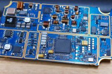
The board seen in post #31 is the FIRST prototype of a high tier police walkie talkie that is now selling, for several K$ each. It works on 4 different frequency bands so it can talk to any other police officer in North America during a large scale emergency. The transmitter runs a single ended GaN fet in class AB for high efficiency. This generates some THD, which is illegal so there is a switched bank of low pass filters (the large air wound coils) to remove the harmonics before feeding the power to the antenna. All harmonics must be 80 dB below the desired signal to be legal.....and you thought home HiFi is clean.
In the first picture the parts in the lower left box are part of the power supply, with the boost inductor, diode, and caps outside the box. The box above that contains some of the transmitter. The GaN fet in on the other side. The largest coil is the drain (parafeed) choke. This feeds the black chip in the box to the right through a small coil and some impedance matching parts (the OPT). The chip is a 4 port switch that selects one of 4 filters which are feeding another 4 port switch on the other side of the board. The large chip in the large box on the lower right is a custom designed CMOS RF chip that our group designed. The purpose of this board was to prove to management that the chip was worth the two years and over one million dollars they spent on it. I had the local PD calls playing on a board like this one when the Chicago bosses came to see it. My prototypes tended to work well, even the early ones like this. That's why I lasted for 41 years in the same company.
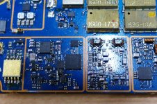
The shiny gold backed square in the lower left box in the second picture is the GaN FET that can make 10 watts of RF power from 100 MHz to over 2 GHz. The flying piece of wire wrap wire bypasses the second stage of a two stage buffer amp that was deemed unnecessary after testing. The 4 brass cans each contain two VCO's to generate all the necessary frequencies needed for the radio. Most of the smaller SMD coils in the box below the VCO's are part of the receiver's filtering. These are needed to keep unwanted signals out of the receiver. TV transmitters use frequencies very close to police radio frequencies. TV transmitters have a radiated power level of up to a MEGAWATT. The Miami Florida antenna farm has 12 of these 1 MW transmitters and some lower powered stuff. Yes, I got away with requesting company funds to test our radios at my favorite worst case test site, the upper deck of the stadium used for the Miami Dolphins and at the time the Miami Marlins. It is 1 mile west of the tower farm.
The upper management ate the megabuck design costs for integrating much of a complex radio into the big chip seen in this board. They then funded the development of a second chip to integrate the 8 VCO's and other frequency synthesizer circuitry. I left the company before the second chip was finished. When the company offered me a box full of money to leave, I took the money and ran.....1200 miles away.
"Standards are such a wonderful thing that everybody has his own".
I am trying convince GM and Toyota to adopt the first 17.5 Inch wheels and tires.
I am trying convince GM and Toyota to adopt the first 17.5 Inch wheels and tires.
That's a really neat design and lots of info, George. Thanks.
The closest thing to RF testing I ever did was find out that if I keyed up a 4W CB radio with the antenna in the same room as the Zenith TV, it would turn the set off and you'd need to unplug it and plug it in again to get it to turn back on. It was kind of a pile of crap though, and 4W of AM is quite a lot of power from 5 feet away.
You can run EasyEDA as a standalone (offline) solution, too. The cloud aspect is just convenient.
Koda, I've done a couple things in EasyEDA. It seems pretty intuitive to me. Are there tube footprints in the library?
I've watched a couple tutorials but they had my head spinning lol.
I've watched a couple tutorials but they had my head spinning lol.
It seems to already be a thing, at least for trailers, maybe medium trucks like the smaller UPS wagons.the first 17.5 Inch wheels and tires.
https://www.google.com/search?q=17.5+Inch+wheels
Yes. Hit Shift-F and search for 12AX7 for b9a etc under "User contributed". There are many to choose from, some are better than others.Koda, I've done a couple things in EasyEDA. It seems pretty intuitive to me. Are there tube footprints in the library?
I've watched a couple tutorials but they had my head spinning lol.
If you need Magnoval, search 6D22S.
Octal search 6SN7 etc
You can click the heart to add them to your favourites to find them easier the next time.
Quite easy.
I should add, that I don't use the circuit/schematic functions, only PCB. I make PCB from scratch and connect the "dots" myself. They do work though.
I have been doing the same for years but using freePCB.I should add, that I don't use the circuit/schematic functions, only PCB. I make PCB from scratch and connect the "dots" myself. They do work though.
Cheers
Ian
I think with most audio work (and RF work) it’s better to just draw the layout of what you need instead of starting with a schematic and trying to make a layout. With most audio amps, you need very specific power and ground routing, keeping some things away from others, keeping right angles between feedback and power, and many things need to have fixed physical placement because you already have the heat sinks drilled and it needs to fit IN THE BOX. You start by placing those critical components, then find a way for everything else to fit and maintain the rules you set up for the design. When you go to multiple GHz, it gets even worse - the layout IS the design. The exact dimensions of all the interconnect are all dependent on one another - change one, it’s reactance changes (and the coupling to everything else changes), you need to retune the entire circuit. To make matters worse the only accurate result is to simulate the entire thing at once with a field solver, which can take anywhere from a few minutes to a few DAYS.
An old primitive PCB package seems to work fine to draw layouts. I do use the schematic features of mine, but never together. Linked schematic/layout always seems to be more of a burden than blessing. To do an LVS you draw the schematic FROM the layout - and you will find any errors. Just do it at least a week or two later. Mistakes become glaringly obvious if you haven’t been looking it the whole time.
An old primitive PCB package seems to work fine to draw layouts. I do use the schematic features of mine, but never together. Linked schematic/layout always seems to be more of a burden than blessing. To do an LVS you draw the schematic FROM the layout - and you will find any errors. Just do it at least a week or two later. Mistakes become glaringly obvious if you haven’t been looking it the whole time.
- Home
- Amplifiers
- Tubes / Valves
- What are the maximum currents I can expect to power a 12AX7?