Hello oloppolo,
please measure the folowing:
R1 and R2: voltage over these two resistors (measured from one leg to the other leg of each resistor)
R21 and R22: voltage over these two resistors (measured from one leg to the other leg of the resistor). The voltage over
R21 and R22 should be extremely low - in the very low mV - region. I assume a slightly higher voltage over R22 - perhaps much higher?
Please report back.
Cheers
Dirk
Hello oloppolo,
these values are excellent. With 22mV over R1 and R2, we know, that the differential inputstage / JFets are biased to 2,2mA.
And now we also know, that all JFets are on.
The values at R21/R22 are also great and well balanced. Now I would assume, that the problem is anywhere in the following stages.
Cheers Dirk
Hello oloppolo,
could you also measure the voltage over resistors R7/R13 and over R11/R12.
Could it be, that your BA2018 linestage works properly and the problem is anywhere else?
When you measured the sinus-signal: how high was the voltage swing of the sinus_signal you were feeding into the input
of your BA2018?
Cheers
Dirk
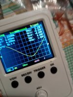
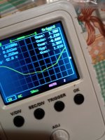
I was confused because one half of the sinusvoltage was cut away and it was asymmetrical voltageswing on the scope.
I thought, that it is perhaps a measurement - mistake. Or one half of the circuit doesn't work properly (positive side)?
Because the values, you have measured on the BA2018 - boards look good (and are symmetrical from positive to negative side).
PSU - 0 V DC / ground at output of PSU is connected to earthground?
I am a litlle bit at my end? Outputstage also biases up (red LED is shining in both channels). Hmmm?
Perhaps some other members have an idea?
Cheers
Dirk
Attachments

Dirk, you got further along than I did!
oloppolo: First, please let us know the answers to Dirk's question in his edited picture. That can help.
Also, now that your boards are out of the chassis, could you post a clear picture of the back side?
Grazie!
oloppolo: First, please let us know the answers to Dirk's question in his edited picture. That can help.
Also, now that your boards are out of the chassis, could you post a clear picture of the back side?
Grazie!
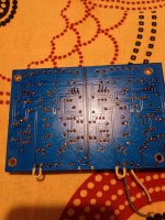

oloppolo: thanks for the pic. I'll dig into it momentarily, but I do see lots of long legs left on some of the transistors. They make me a bit nervous! Is there any chance they are touching the chassis when the board is mounted inside?
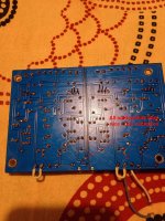

Don't if it could be a "bridge" or just some dirt/hair (picture)?
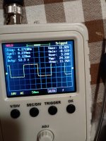
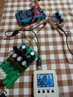
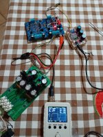
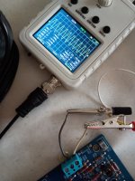
Could it be an idea to use scope to look at signal from input and then follow the signal in path from input to output and see when signal start to look bad?
Assume you see a perfect sinus at board input?
Could it be an idea to use scope to look at signal from input and then follow the signal in path from input to output and see when signal start to look bad?
Assume you see a perfect sinus at board input?
Attachments

Your circuit board is probably OK considering all the measurements you've supplied when requested.
Try a 10K ohm resistor across the output terminals, short the input and verify the DC offset adjustment. Then put the signal generator to the input and put the scope leads across the 10K load resistor. I like to see what the output measures and looks like loaded.
Try a 10K ohm resistor across the output terminals, short the input and verify the DC offset adjustment. Then put the signal generator to the input and put the scope leads across the 10K load resistor. I like to see what the output measures and looks like loaded.
How much A/C voltage is your signal generator producing? If the in- to gnd connection is cut, then the preamp is amplifying less.
This was one of my questions above. If the signal generator is overdriving the input...
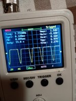
But on the scope it looks asymmetrically clipping. As if anything is not referenced to audioground?...
Cheers
Dirk
But on the scope it looks asymmetrically clipping. As if anything is not referenced to audioground?...
Cheers
Dirk
- Home
- Amplifiers
- Pass Labs
- Wayne's BA 2018 linestage