I cannot overstate how important this is, especially given the loads we are often powering. If you are aiming for 0.00xx Ω and 0.XXnV, (*You can keep it compact, particularly if its only a low voltage, low current load and you dont need significant heatsinking), distance is the enemy; remote sensing (if implemented) and feedback can only do so much.Keep the PCB as small as possible so that it can be placed as close as possible to the load itself.
Yes, agreed, giving it its own secondary is preferred.
Preferably you have minimal input/bypass caps on the load, for stability
Last edited:
Hello. yes it is actually possible to put smaller heatsinks and reduce the size of the circuit, I chose to have the rectifier on the PCB to have the possibility to compact the assembly on the box, and make it as modular as possible, we will also have the possibility to omit it by breaking the PCB and reduce it even more.Keep the PCB as small as possible so that it can be placed as close as possible to the load itself. It is not necessary to have a rectifier on the PCB.
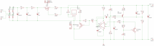
On this version with GLED431 and jfet CCS the serial transistor has no heatsink at all, and for the input CCS only a small PCB serves as a heatsink. The voltage drop on the regulator is only 4V so BSP149 was used instead of DN2540.
Nice progress!
Just a couple thoughts….
How hot do the heatsinked parts get? My concern would be they are very close to the electrolytic caps. Also, if they were turned 90° so the backsides face outwards the hardware to attach the heatsinks would be more accessible.
Just a couple thoughts….
How hot do the heatsinked parts get? My concern would be they are very close to the electrolytic caps. Also, if they were turned 90° so the backsides face outwards the hardware to attach the heatsinks would be more accessible.
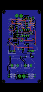
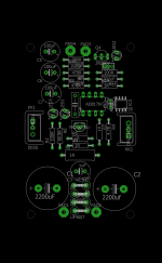
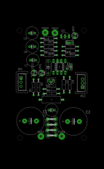
Tix88, small guidelines from me, this is my last PCB for WJ shunt, dimensions are 40X30mm, single sided PCB with ground plane.
I had already added CCS with 2SK246 for LM4040 which was later replaced with GLED431. Also the 100uF located next to the LM4040 should be UKZ 100uF / 25V so it needs a little more space.
I had already added CCS with 2SK246 for LM4040 which was later replaced with GLED431. Also the 100uF located next to the LM4040 should be UKZ 100uF / 25V so it needs a little more space.
Attachments

Good suggestions. He will try to remove the heat sink caps.Nice progress!
Just a couple thoughts….
How hot do the heatsinked parts get? My concern would be they are very close to the electrolytic caps. Also, if they were turned 90° so the backsides face outwards the hardware to attach the heatsinks would be more accessible.
Good ideas thanks. I will try to optimize the arrangement of the components, but they are already at the size limit. the only way to further decrease the size would be to use SMD partsTix88, small guidelines from me, this is my last PCB for WJ shunt, dimensions are 40X30mm, single sided PCB with ground plane.
I had already added CCS with 2SK246 for LM4040 which was later replaced with GLED431. Also the 100uF located next to the LM4040 should be UKZ 100uF / 25V so it needs a little more space.
Here is the latest version of the pcb, I have moved the components of the caps as much as possible, and I have reduced the size even more. I add the smd opamp.
Attachments

Last edited:
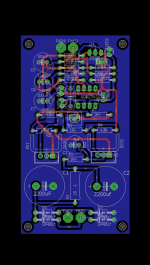
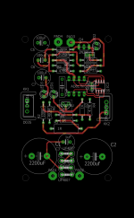
Final PCB for the positive part of the shunt. I inserted the smd opamp inside the non-smd one to shorten the connections, I attach the original files so those who wish can have it printed independently, or modify it according to their needs. I will send the first 5 pieces to print, to test it if everything is correct and there are no errors, after which the pcb project will be completed.
Attachments
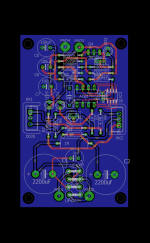
Hi, here are the pcb files, positive and negative. They are not tested and are waiting for the pcbs to be able to carry out the first test and see if everything is working, so try at your own risk.
Attachments

Hi everyone.
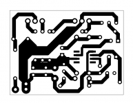
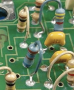
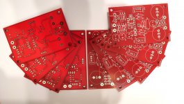
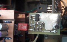
Finally the pcbs have arrived, as you can see from the photo they also look nice.
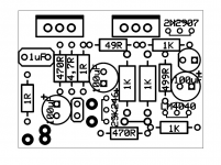
I noticed 2 problems with the pcbs
1) The footprint for the opamp is bigger than that of the opamp1641 that I bought from mouser, and therefore I will need to use an adapter in this first step
2) the distance used for the resistors is not compatible with the vishay rn60 series resistors because these are larger in diameter and cannot be mounted well, but you have to opt for a cantilever mounting. For normal 1 / 4w resistors the distance is correct
These two problems will be solved in the new version of pcb that I will create when the testing of this in my possession is completed.
I am proceeding with the assembly of the components on the pcb to proceed with the first test.
I realized that I forgot to purchase the 2n2907 component, what possible common replacement could I use?
Finally the pcbs have arrived, as you can see from the photo they also look nice.
I noticed 2 problems with the pcbs
1) The footprint for the opamp is bigger than that of the opamp1641 that I bought from mouser, and therefore I will need to use an adapter in this first step
2) the distance used for the resistors is not compatible with the vishay rn60 series resistors because these are larger in diameter and cannot be mounted well, but you have to opt for a cantilever mounting. For normal 1 / 4w resistors the distance is correct
These two problems will be solved in the new version of pcb that I will create when the testing of this in my possession is completed.
I am proceeding with the assembly of the components on the pcb to proceed with the first test.
I realized that I forgot to purchase the 2n2907 component, what possible common replacement could I use?
Attachments
Good job Tix88, regardless of the problems, although I would like the PCBs to be smaller, with shorter traces and no rectifier. Here are a few ideas for new PCBs.Hi everyone.
Finally the pcbs have arrived, as you can see from the photo they also look nice.
I noticed 2 problems with the pcbs
1) The footprint for the opamp is bigger than that of the opamp1641 that I bought from mouser, and therefore I will need to use an adapter in this first step
2) the distance used for the resistors is not compatible with the vishay rn60 series resistors because these are larger in diameter and cannot be mounted well, but you have to opt for a cantilever mounting. For normal 1 / 4w resistors the distance is correct
These two problems will be solved in the new version of pcb that I will create when the testing of this in my possession is completed.
I am proceeding with the assembly of the components on the pcb to proceed with the first test.
I realized that I forgot to purchase the 2n2907 component, what possible common replacement could I use?
I installed a new input CCS (BSP149, BSS159) yesterday, I also changed the CCS for GLED431 with BSS139 delpetion mosfet, both changes improved the regulator feature. I used BSP149 because I have a voltage drop of only 4V so there is not much dissipation on it.
Instead of 2N2907 (PN2907) I used BC327 or 2SA1015 and you can use any PNP in TO92 with higher Ic. Just watch the pin layout.
Attachments
Hello everyone, finally after the summer holidays to various adventures in life I was able to put my hand to the circuit to test it. I powered the circuit and it seems to work, all the LEDs light up normally, when empty I have a voltage of 7.5v, but when I connect a 100ohm resistor to the output, 2 LEDs go out and the output voltage drops to 2.5V, and I don't copy what the reason is.
I measured the values, but there is something wrong@Tix88 did you measure the current through the CCS (voltage drop on R4)?
If R11 and R12 are 1K then the output voltage should be 5V if GLED431 and Q4 are working properly. You must have 2.5V on the R9.
on the R4 I measure 44.5mV and on the R9 I measure 0.8V.
@Tix88,something is definitely wrong, the voltage drop across R4 must be around 0.5V. It seems that the GLED431 is not working properly either, what is the voltage drop on R13? R10 must be 150R. What op.amp did you use? What is the voltage before the DN2540 itself?I measured the values, but there is something wrong
on the R4 I measure 44.5mV and on the R9 I measure 0.8V.
According to your measurements, the current is only 10mA, which is 10 times less than necessary.
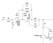
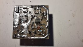
In the meantime, I finished a new prototype PCB, DN2540 was replaced by CPC3902 in cascade with BSS139, BSS139 in cascade was also used for reference, op.amp is AD817 but I will soon replace it with ADA4896.
Attachments
Hello. I use an OPA1641, on the R13 I measured 1.2V. before the dn2540 I measure 11.5V@Tix88,something is definitely wrong, the voltage drop across R4 must be around 0.5V. It seems that the GLED431 is not working properly either, what is the voltage drop on R13? R10 must be 150R. What op.amp did you use? What is the voltage before the DN2540 itself?
According to your measurements, the current is only 10mA, which is 10 times less than necessary.
In the meantime, I finished a new prototype PCB, DN2540 was replaced by CPC3902 in cascade with BSS139, BSS139 in cascade was also used for reference, op.amp is AD817 but I will soon replace it with ADA4896.
- Home
- Amplifiers
- Power Supplies
- Walt Jung shunt Design