If you keep the VAS current in the KSA1381/KSC3503 pair in the range that Lazy Cat and Shaan have suggested, 10~15mA then you do not have to do much until you get to +/-45V supply. Just recalibrate at the higher voltage.Hi Pete,
My intention initially is to use it on 37v rails but I may want to try it on higher rails later. What would need to be changed so it could be used at higher rails?
Thanks, Terry
As the supply voltage or VAS bias current increases, the power dissipated in the VAS transistors rises. At some point, the small top-side heatsinks will get too hot. Then you have to use the option to mount the transistors under the board, on the main heatsink.
Above 45V, a different input transistor pair rated at a higher voltage, and possibly other component value changes.
If you keep the VAS current in the KSA1381/KSC3503 pair in the range that Lazy Cat and Shaan have suggested, 10~15mA then you do not have to do much until you get to +/-45V supply. Just recalibrate at the higher voltage.
As the supply voltage or VAS bias current increases, the power dissipated in the VAS transistors rises. At some point, the small top-side heatsinks will get too hot. Then you have to use the option to mount the transistors under the board, on the main heatsink.
Above 45V, a different input transistor pair rated at a higher voltage, and possibly other component value changes.
Am I correct in understanding that the pots in your design control the VAS current? Any advantage in running the VAS at a higher current and attaching the VAS transistors to the main heatsink?
Indirectly, yes. The trim pots control the CCS current, and indirectly the VAS current. There is a good explanation somewhere in the main VSSA thread.Am I correct in understanding that the pots in your design control the VAS current? Any advantage in running the VAS at a higher current and attaching the VAS transistors to the main heatsink?
Opinions on the VAS bias current differ. Probably because "best" is likely to be different for different VAS transistors, and there are several in use. I set mine close to what Lazy Cat and Shaan have suggested.
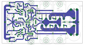
This is the way to build it!
Hi PMI!!! To be honest...I like your design better😉. I never liked the SMD.
I know your boards are bigger, but that is the way to go!
Very good job!!!!
Hi PMI!!! To be honest...I like your design better😉. I never liked the SMD.
I know your boards are bigger, but that is the way to go!
Very good job!!!!
Hello,
I saw a few posts stating they wanted PCBs for your VSSA Through-Hole PCB. I would like to get 4 boards for 2 amps.
Please let me know if there is another place where I can ask for this as I didn't see it in the group buy section.
Thanks.
Bertrand
I saw a few posts stating they wanted PCBs for your VSSA Through-Hole PCB. I would like to get 4 boards for 2 amps.
Please let me know if there is another place where I can ask for this as I didn't see it in the group buy section.
Thanks.
Bertrand
"This revision diverged from the original PeeCeeBee topic too much to post the technical details there - however, my intent is to let anyone interested to etch the board from a pdf file, and build it with the simple components that Shaan proposed."
Waiting for pdf.....🙂
Waiting for pdf.....🙂
@lanchile:  thanks, 🙂
@Royber: You were already on the list. 😀
@Tome: Done, added your name.
@thimios: As soon as I am done testing, it will be posted. That will take a few days. Schematic and BOM are being reviewed and updated.
I have a list of names of those interested in boards from the other thread, anyone who wants to add their name, please just make a one-line post. If there are more than a few more, I will open a thread in the GB section, but that will not be for a few days.
thanks, 🙂@Royber: You were already on the list. 😀
@Tome: Done, added your name.
@thimios: As soon as I am done testing, it will be posted. That will take a few days. Schematic and BOM are being reviewed and updated.
I have a list of names of those interested in boards from the other thread, anyone who wants to add their name, please just make a one-line post. If there are more than a few more, I will open a thread in the GB section, but that will not be for a few days.
@lanchile:
@Royber: You were already on the list. 😀
@Tome: Done, added your name.
@thimios: As soon as I am done testing, it will be posted. That will take a few days. Schematic and BOM are being reviewed and updated.
I have a list of names of those interested in boards from the other thread, anyone who wants to add their name, please just make a one-line post. If there are more than a few more, I will open a thread in the GB section, but that will not be for a few days.
Thanks! Does it show that I really really want this? hehehe.
Bertrand
Stimulating some discussion...
PMI was hoping to make this a build and discussion thread, so rather than simply watch it plug up with requests for the goods (the PCB's that is) let's begin some active discussion.
I'd like to open perhaps with some discussion on the front end, specifically the transistor choice for the input pair and the CCSs that feed them current. We can also touch on the input coupling and filter section as well since some recent comments suggest there may be some value in adjusting these.
First off, I'm not sure which transistors have already been used by others aside from the ever popular BC550C / BC560C and my use of 2SA965 / 2SC2235 in my initial 'junk box' PeeCeeBee and then moving to some 2SA992F / 2SC1845F for better parameters like higher hFE and lower Cob. Any others we should be exploring actively?
I have personally done very little with JFETs. What are the current recommendations and selection criteria? I know we need and IDSS at least a little higher than our target for self bias with a reasonable source resistor value and a suitable Vds rating for starters.
Finally, the current values of the input band limiting filter set the high frequency corner at 1.6MHz. It has been noted that this is quite high. Would a lower limit more like 200kHz (10x the audio band) be more suitable?
I suggest we work at least somewhat methodically through the circuit to see how we can best optimize it with prudent active component selection and value changes of passives if warranted. It would be still nice to avoid difficult to source parts as was one of the goals back in the PeeCeeBee thread.
Let's get some meaningful discussion going! Pete, if I'm out of place here just say so.
Last edited:
Pete, I'll wait for your higher voltage test 🙂 with single pair output...If you keep the VAS current in the KSA1381/KSC3503 pair in the range that Lazy Cat and Shaan have suggested, 10~15mA then you do not have to do much until you get to +/-45V supply. Just recalibrate at the higher voltage.
As the supply voltage or VAS bias current increases, the power dissipated in the VAS transistors rises. At some point, the small top-side heatsinks will get too hot. Then you have to use the option to mount the transistors under the board, on the main heatsink.
Above 45V, a different input transistor pair rated at a higher voltage, and possibly other component value changes.
yes the VAS will be so hot & I don't like that hot, they are only 5-7w device
My 2 pairs output show instability with more than +/-40VDC.
It was 52VDC😀 & the negative rail show something wrong 😱...
I use 120V transistor for input pair & no CCS yet, maybe should add CCS instead resistor also some component value must be changed
(like you suggested at PeeCeeBee thread)
Maybe my boards not good enough too

For anyone who will build higher voltage version,
please be careful & I like to know the result.
Jason,
yes about the CCS, I'm waiting too 🙂
but I will try with what I have, see if 2SK246 can be used.
Regards
Last edited:
I have not had any problems at +/-45V. I can't run at 50V until I build the next pair of test boards with different input transistors, and higher rated feedback resistors.Pete, I'll wait for your higher voltage test 🙂 with single pair output...
yes the VAS will be so hot & I don't like that hot, they are only 5-7w device
My 2 pairs output show instability with more than +/-40VDC...
Most of my measurements are taken at lower voltages, basically for convenience, but after your last post, I ran a few quick tests, using a bigger transformer (400VA) and a Variac. No measurements taken, just a few tests, because full power at 45V can't be sustained for long with what I have.
The waveforms do not look much different than at 30V. I ran up to clipping at 1KHz, 10KHz, and 50KHz, sines and squares, each test about 30~40 seconds, unloaded and loaded, checked the slew rate, etc.
Clipping behavior is nice and controlled, you could almost call it "soft" clipping.
I set the VAS bias to 12 mA at 30V, and with the CCS, it increases to about 15mA at 45V. I did not take the time to recalibrate at 45V.
No instability noted.
If anything, the 10 and 50KHz square waves look better loaded than unloaded, because there is no overshoot on the leading and trailing edges. This leads me to think the input filter bandwidth is set unnecessarily high (more on this later).
PMI was hoping to make this a build and discussion thread, so rather than simply watch it plug up with requests for the goods (the PCB's that is) let's begin some active discussion.
I'd like to open perhaps with some discussion on the front end, specifically the transistor choice for the input pair and the CCSs that feed them current. We can also touch on the input coupling and filter section as well since some recent comments suggest there may be some value in adjusting these.
First off, I'm not sure which transistors have already been used by others aside from the ever popular BC550C / BC560C and my use of 2SA965 / 2SC2235 in my initial 'junk box' PeeCeeBee and then moving to some 2SA992F / 2SC1845F for better parameters like higher hFE and lower Cob. Any others we should be exploring actively?
I have personally done very little with JFETs. What are the current recommendations and selection criteria? I know we need and IDSS at least a little higher than our target for self bias with a reasonable source resistor value and a suitable Vds rating for starters.
Finally, the current values of the input band limiting filter set the high frequency corner at 1.6MHz. It has been noted that this is quite high. Would a lower limit more like 200kHz (10x the audio band) be more suitable?
I suggest we work at least somewhat methodically through the circuit to see how we can best optimize it with prudent active component selection and value changes of passives if warranted. It would be still nice to avoid difficult to source parts as was one of the goals back in the PeeCeeBee thread.
Let's get some meaningful discussion going! Pete, if I'm out of place here just say so.
If I may, I can add some thoughts about this, in the light of my new future build, the balanced VSSA.
For CCS, there are choices of using bipolar transistors, degenerated JFETs or CRDs. One CRD at 2,4mA is Siliconix J508 produced also by Linear Systems. The disadvantage is +/-20% tolerance and lack of adjustment possibility. So you have to buy more and sort them out.
For JFETs, you can use series resistor if you want to go higher on voltage. In VSSA modules, the useful adjustment range is quite thin. On the sweet spot rotating the trimmer 15 degrees can throw you out of the range. This is something that should be worked out, I would say.
A current mirror with Bc546/556 is also something to be taken into account, especially for higher voltages. Or why not, even better 2SA970/2SC2240.
For input transistors,2SA992/2SC1845 seem to be a good choice for higher voltages. For lower voltages we could aim for higher hfe transistors, but I have no clue at the moment if for example the obsolete NPN MPSA18 has a PNP counterpart. The hFE for this one can be as high as 1500. Maybe somebody has an idea.
In my build I will use BC550C/BC560C as I will supply the stages at 80V (+/-40V equivalent).
As VAS transistors I will use 2SA1142/2SC2682 with a Cob=4,5pF and fT=180MHz; the problem with these is poor matching, 4 usable pairs (+/-5%) out of 30. Another option would be 2SA1360/2SC3423, with even lower Cob (2,5pF) but I didn't explore them about match-ability. I know others were discussed as well.
Other strong suggestion (quite obvious for some people lurking around these threads) is to use a cap multiplier. The one designed by MrEvil and improved for this purpose by Pete is fabulous in efficiency. The visible ripple on the storage caps (even while using 2x15.000uF on every rail) is completely vanished after the CM. It's difficult (but not impossible) to use it over +/-50V, due to the limitations in the voltage the components can take. I found IRFB4410 that can take 100V with 96A maximum current and 8mOhms Rds(on) resistance; so there is hope 😀
Cheers!
(Pete, please let me know as well if this discussion is off-topic/unwanted in this thread)
All component discussion and suggestion are welcome... 😀
Having said that...
I am testing with the following components, so take this as a starting point:
@Metallicus: I believe I have the components for a higher voltage version in hand now, just have not had time to test.
Having said that...
I am testing with the following components, so take this as a starting point:
- 1K and 100pf in the input filter. This gives some impressive test results with 50K~100K Hz square wave, but for a practical amplifier, 2.2K and 220pf is more realistic.
- BC550C/560C, mainly just to compatible with LC's design. I have also received a few hundred old stock BC546C/BC556C from another member, both for this project and for Bonsai's nx-Amp. Other alternatives are welcome.
- J112 N-channel Jfet in the CCS circuit, with 2K trim pot to adjust the current, and a 3.3K~5.6K series resistor to limit the voltage at the Jfet. Unless a better alternative emerges, I plan to ship a pair of these with every board.
- KSA1381E/KSC3503E VAS transistors. They are fairly easy to match, and because the KSC3503E is obsolete and hard to get now, I plan to supply a set to anyone who wants to use these, at least for the first few dozen boards. I am open to other suggestions.
- MrEvil's Cap Multiplier PSU. It took me a long time to settle on that one, and frankly I was surprised more people did not jump on this before. It is a very cool circuit, and produces much cleaner power with one pair of 10.000uFd caps than an expensive capacitor bank in CRC configuration.
@Metallicus: I believe I have the components for a higher voltage version in hand now, just have not had time to test.
Added to the list, 🙂Hi PMI
2 boards for me please
thanks
kp93300
Power supply
Hello,
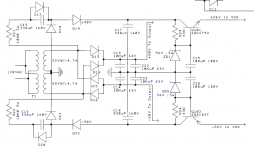
There has been some discussion around the power supply and I would like to show one potent option for it.
It has been shamelessly stolen from Steven Dunlap´s Krill schematic. I have used this type of supply with other amp projects with great success. Of course you may need to adjust some of the values according to the desired attenuation for input/vas. You may even add fancier regulator after the zener/transistor regulator.
Jarno
Hello,
There has been some discussion around the power supply and I would like to show one potent option for it.
It has been shamelessly stolen from Steven Dunlap´s Krill schematic. I have used this type of supply with other amp projects with great success. Of course you may need to adjust some of the values according to the desired attenuation for input/vas. You may even add fancier regulator after the zener/transistor regulator.
Jarno
Attachments
- Home
- Amplifiers
- Solid State
- VSSA Through-Hole-PCB build thread