So is this the never ending GB or are these going to be mailed our some day? 😀
Please send an e-mail to Semelab, UK, and tell them that a lot of people are waitng for ALF08NP16V5. You see why VSSA PCB sets are on hold, although VSSA PCBs are assembled, sealed and waiting here.
In April 2013 I ordered 300 pcs., 185 received, the rest 115 are on back order waiting to be delivered as soon as they will be produced. Up to now they postponed delivery for five times, and this is the fact. Please send some apeal to Semelab, maybe it would help.
Best regards to all, Andrej

Last edited:
VSSA could not be overcome so easily, guys tried in many threads, but so far unsuccessfully. The only possibly one will be the First One if ...BTW, based on my experience with the PeeCeeBee version it is worth waiting for.

Keep-it simple is, indeed, VERY difficult 🙂VSSA could not be overcome so easily
where is the explanation of how the vssa works. It was in a link at one point in time, but i cant seem to find it.
Hi buzzforb
Your old request Look post 1869, imagine you maybe hurry too much for finding.
Also maybe interesting for others waiting last batch from semelab when they gets quality die to make produktion. Post 1869 holds four pages of first Installation manual that belongs to the commercial layout version from Andrej.
PCB needs corrections:
1 - Short R23
2 - If high inrush current from PSU read SMPS, replace R19, R20 with Farnell MPCWR10FTFQ100
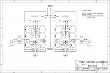
3 - I attach VSSA grounding schematic as jpg-image from another post cant remember but attach here.
4 - In Step 2 of Calibration adjustments in Installation manual the correct text should be as follows: "Our final target for V-meter 1 reading is 4,00 V and 0 mV for V-meter 2 reading. Turn on the power supply and observe both V-meters displayed values. Clockwise rotation of TR3 will increase V value of V-meter 1 and should have no effect on mV value of V-meter 2 readings. Rotate trimmer TR3 in a direction to reach our final target goal 4,00 V reading on V-meter 1 (meaning 4,00 V/22 Ohm = 182 mA output bias current + front end bias current)."
BR Ricky
Your old request Look post 1869, imagine you maybe hurry too much for finding.
Also maybe interesting for others waiting last batch from semelab when they gets quality die to make produktion. Post 1869 holds four pages of first Installation manual that belongs to the commercial layout version from Andrej.
PCB needs corrections:
1 - Short R23
2 - If high inrush current from PSU read SMPS, replace R19, R20 with Farnell MPCWR10FTFQ100
3 - I attach VSSA grounding schematic as jpg-image from another post cant remember but attach here.
4 - In Step 2 of Calibration adjustments in Installation manual the correct text should be as follows: "Our final target for V-meter 1 reading is 4,00 V and 0 mV for V-meter 2 reading. Turn on the power supply and observe both V-meters displayed values. Clockwise rotation of TR3 will increase V value of V-meter 1 and should have no effect on mV value of V-meter 2 readings. Rotate trimmer TR3 in a direction to reach our final target goal 4,00 V reading on V-meter 1 (meaning 4,00 V/22 Ohm = 182 mA output bias current + front end bias current)."
BR Ricky
Attachments
Last edited:
Actually, that is the setup procedure. I was asking about an explanation of how the configuration works. I believe Nico Ras had it in his signature at one point, but it is no longer there. THinking about using this as driver for buffer output stage, but was wandering about gain setting.
Hi Again buzzforb
Saw you had VSSA for sale at moment, have you ever had VSSA modules set up and made listening test? if i dont think you have made us share listening ?
BR Ricky
Saw you had VSSA for sale at moment, have you ever had VSSA modules set up and made listening test? if i dont think you have made us share listening ?
BR Ricky
I home etched the Renesas lateral version. Did not build the PCB version. It is a good amp, but I wold choose the TSSA1.6. Full disclodure. I did not try with SMPS or Exicon dual fets. I want to try the SSA as well.
Actually, that is the setup procedure. I was asking about an explanation of how the configuration works.
I can try to answer, under L.C. control...
First it is a Current feedback amplifier. Means it don't use a symmetrical long tailored pair to cancel the distortions, but a simple transistor (two because symmetrical).
While the signal get in in the base (there the input transistor acts as common emitter) in relatively hight impedance, the feedback is applied at its emitter, at low impedance. The transistor works in common base for the feedback.
The advantage of this is the combination of low impedance and reduced parasitic capacitance of the emitter, compared to its base, increase the bandwidth of the feedback signal and the slew rate, giving a better transient behavior, on my believes. Because it minimize the HF phase turns in the feedback, before it is compared to the original signal.
The negative point is the input transistor's distortions are not canceled in any way, comparing to an LTP.
There is a second inconvenient of this configuration: the ~0.6 diode drop voltages in the base-emitter junctions. This makes DC coupling of both input and feedback impossible in the same time.
Setting the input transistors base at 0V allow direct coupling of the input signal.
Dividing the feedback paths in two symmetrical networks (-0.6V+06V =0V) allow them to cancel themselves those voltages drops in the opposite point where the serial resistances are connected together. You can now connect them to the 0V DC output with no DC error, allowing DC operation of the feedback.
The input stages give a current gain and has been carefully feed in current by 2 constant current source in order to minimize their distortions and sensitivity to rail ripples. The two inputs transistors are glued together to minimize their temperature differences, ie offset variation.
The following stage acts as both voltage amplification (VAS) and driver, to provide a signal with enough level and current to can drive the power lateral mosfets and their high parasitic gate capacitances.
As both the VAS and the mosfets are in the closed loop, their own distortions are canceled by the feedback.
I believe the fact that ALFs are build with both devices in the same DIE contribute to reduce their temperature delta for both transients and bias, making this amp having an offset low enough and stable enough to get rid of any DC servo.
As the schematic use only 3 poles, each device very fast, low impedances everywhere good for HF and protection against parasitic capacitances, as well as SMD and compact board design, minimizing parasitic inductances, this amp offer a very wide bandwidth, a very nice high slew rate, as well as a high stability margin.
Last point is the sensibility of Current feedback amplifiers to power supply ripples. (LTP cancel them in VFA) . LC has kept great care to filter them, as you can see in the rails paths, all along with the constant current sources.
The end of the story is the talent of L.C., to set the current and gain of each stage at their best to minimize distortions and optimize each pole cutoff. Both with the help of measuring instruments and listening,
Listening is the most important step, often neglected by designers.
This little amp is obviously designed for music reproduction, not as an operational amplifier, while i believe he measure quite well for so few parts.
It fulfill one of the most difficult goal to reach: Keep It Simple. Make-it sound easy and transparent.
L.C you are, of course, free to correct and complete this short and naive analyze.
Last edited:
@Esperado: Gluing the input transistors is fairly easy (I've done that), but I wonder about the normal variation in the NPN-PNP pairs. On my through hole boards made from Shaan's schematic, I used matched transistors. On LC's original VSSA, I just installed those that came with the modules, and I noticed that the offset adjustment was very sensitive, and the offset drifts with temperature.
Meaning, a tiny fraction of a turn on the trim pots changed the offset by a large amount (input shorted for adjustment). Is this because the diode drops have to cancel each other exactly, or is something else going on?
Meaning, a tiny fraction of a turn on the trim pots changed the offset by a large amount (input shorted for adjustment). Is this because the diode drops have to cancel each other exactly, or is something else going on?
Transconductance of transistors are not linear and very sensitive to temperature.Meaning, a tiny fraction of a turn on the trim pots changed the offset by a large amount (input shorted for adjustment). Is this because the diode drops have to cancel each other exactly, or is something else going on?
If your trim is too sensitive, you can use a lower value + one resistance on each side, for the total make the same value. Just try to measure in witch range of values you are in various temperatures and adjustments, and keep a little more margin for your trim stay side to side inside those values. I don't know if i make myself clear.
In the previous description, i forgot to precise that the input stage provide yet a x10 voltage gain (470/47 ohms) to the signal. Low enough, in regard to the total gain of the transistor to keep a low distortion factor. Too late to edit.I can try to answer, under L.C. control...
And to precise that the mosfet used as power devices are lateral, means they have a negative temperature curve, making unnecessary to add any compensation temperature network to avoid quiescent current run out, with their evils. The quiecent current has been set enough to provide a Class A working condition in normal listening levels, and, i suppose, near the point where transconductance/temperature curve is flat.
Last edited:
Hi Christophe thanks for Words post 2190, you are good at explaining for hobbyist level to understand.
I have question if you have time concerning the decoubling the 2200uF-elko/10uF-Film set combo does for the feedback from output stage. When simulating the groupdelay down lows lags if scaling into mili/micro/nano seconds. So i found one huge capicitance Nichicon 22f Ø12,5xL31,5 5mm lead Space at fair expence which minimize groupdelay errors in simulation. You earlyer in post 1451 gave a practice to find decoupling film cap of the induktor effekt in big elkos. Can you guide me for a suggest maybe i shall use the huge one plus small elko plus film cap ? The huge one has ESR 0,3ohm DCR 0,4ohm. Is rated 2,7v Andrej claims 1v is enough. Can you guide if its worth.
BR Ricky
Not sure if you agree that unmatched Vbe, or something similar may be causing this, or if you are telling me I am barking up the wrong tree... 😀😉 The offset change is not linear to the rotation of the trim pot.Transconductance of transistors are not linear and very sensitive to temperature.
If the BC550/560 are the problem, replacing those with a more closely matched pair would be easier than dealing with the SMD components in the center of the board... I thought of that, but... 😱 ... a bit hard to do, because I will have to remove the 2200uF caps to get to the trim pots, and even then, this would not be easy. To be honest, I am reluctant to change SMD parts on the modules with, or without a matching schematic.
PMI and buzzforb did you guys ever listened to VSSA modules, I mean originals from GB? I don't remember reading anything about your impressions. Others variants don't count cause they cannot be comparable, first reason is the layout, etc.
Yes, of course I have listened to the modules... and I am not planning to hack up your SMD board any time soon, if ever, not to worry. 😀PMI and buzzforb did you guys ever listened to VSSA modules, I mean originals from GB? I don't remember reading anything about your impressions. Others variants don't count cause they cannot be comparable, first reason is the layout, etc.
I am just trying to understand what Esperado is telling me, and in my case, the "understanding" part can take a bit longer than the "listening" part. Not everyone can just look at a circuit on paper, and know how it works immediately, some of the rest of us have to work hard just reading along with the class... 🙄
I'm not sure to understand. I don't see any offset trimming pot in the VSSA L.C. schematic.If the BC550/560 are the problem,
Only one for the quiescent current. If your offset is too important, yes, you can try better matched transistors.
From a theoretical point of view, yes, unpaired devices both higher the offset and the variation of it with temperature.
Last edited:
OK, we are on the same page then, I just wanted to make sure.I'm not sure to understand. I don't see any offset trimming pot in the VSSA L.C. schematic.
Only one for the quiescent current. If your offset is too important, yes, you can try better matched transistors.
From a theoretical point of view, yes, unpaired devices both higher the offset and the variation of it with temperature.
There are three trim pots on the module, two in addition to the schematic. Those two change the front end offset and the bias at the same time. Those are very touchy (sensitive to small rotation) They can be very difficult to set so bias is as specified, and offset is close to zero at the same time. The test points are behind the main filter caps, and there is nothing to clip on (unfortunately I trimmed the VAS transistor leads b/f I tried setting the bias), so it becomes a three-hand operation.
edit for clarification: Can't remember exactly, it's been a couple weeks since I first set everything up. I checked the offset and trim pots again a few days ago (using a better/newer voltmeter), and my question was in reference to what I saw, and to your explanation about the two transistor diode drops cancelling each other.
(I'll shut up now, but thanks for the insight... 😀)
Last edited:
- Home
- Vendor's Bazaar
- VSSA Lateral MosFet Amplifier