My recommendation(s) would be:
One way -
One way -
Read post 1
Read this thread - https://www.diyaudio.com/community/...-walkthrough-featuring-the-fab-jlcpcb.404905/
Another way -Ask in the swap meet
There are likely a number of other ways.Doesn't seem like you have missed anything. Also: The usual minimum load for these regs is around 10mA, so 20mA is more or less still just idling 🙂Am I correct that an LM317/337 chip passing say 20mA doesn't need a heatsink?
By my calculations:
P = EI = 5v drop across the regulator x 0.02A = 0.1W
According to the data sheets for the recommended On Semi Reg The Thermal resistance from Junction to Ambient is 65C/W
Therefore 0.1W with no heatsink would be 0.1w x 65C/W = 6.5C Rise above ambient?
Have I missed anything?
I had PCBs made a while ago and may have a couple. I'd be happy to have another batch made to share. But I don't seem to have the Gerbers anymore.

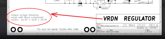
I finished building my VRDN but only have 9 and 12 volt transformers handy to try it out with. It seems to be working well but I notice that the potentiometers don't seem to have any effect on the output voltage. Could that be because I am running the power supply at a lower voltage than it was designed for?
Okay and thanks Rick, I was afraid I had screwed something up in the build. Will try to lay my hands on a higher voltage transformer. I had hoped when I built this that I could use it's adjustability to use it as a multi-purpose power supply to power devices in the 5-15 volt range with an appropriate transformer but that won't work if the adjustibility goes away at lower voltages.
I had hoped when I built this that I could use it's adjustability to use it as a multi-purpose power supply to power devices in the 5-15 volt range
Check the schematic attached to post #1 of this thread. Also check the thread title, VRDN: bipolar regulator PCB for line level ckts: ±11V to ±20V @ 1.5A with "De-Noiser"
_
Attachments
I was in no way blaming you Mark, you are absolutely correct and I saw those but this being DIY I thought there might be some wiggle room. All part of the learning process.
PS- maybe some day you might consider designing one of these for those of us who want to build our own linear power supplies to power our dacs and routers and other devices that work in that 5-16 volt range. One with adjustible voltage would be really appreciated since it could be moved around in search of where it does the most good for sound quality in a system.
PS- maybe some day you might consider designing one of these for those of us who want to build our own linear power supplies to power our dacs and routers and other devices that work in that 5-16 volt range. One with adjustible voltage would be really appreciated since it could be moved around in search of where it does the most good for sound quality in a system.
If you're looking for something for lower voltages, you might try this:
https://www.amb.org/audio/sigma11/
Easy to build.
https://www.amb.org/audio/sigma11/
Easy to build.
If anyone is interested, I have a bunch of VRDN boards in the swap meet for very cheap as I ordered a lot.

- Blue PCB
- HASL Finish
- 2 oz outer copper
- 1.6mm board thickness
Last edited:
I am using three VRDNs for my BA2018. (One for each channel and one for a Muses setup.) All three will be hanging off of a single Antek AS-0518 transformer. Each VRDN contains secondary snubbers: (MOV1, C1, R1) and (MOV2, C2, R2). Built with the recommended parts, C1 is 0.68uF and R1 is 39R. C1 and R1 are the same as C2 and R2, respectively. The MOV parts are 400pF or 500pF (0.0004uF or 0.0005uF) depending on the spec sheet you find.
I started wondering about the effect three VRDNs would have since they were all going to be hanging off of one transformer, and what the total combined snubber values might be. In the "Quasimodo results (ONLY)" thread, the posted values for the AS-0518 transformer are:
Cx = .01uF
Cs = .15uF
Rs = 44.2Ω
The three VRDNs seem to me to be in parallel to each other in my system. If that is the case, then the snubber circuits are as well. So for one secondary from the transformer, the combined stock snubbers would give these values:
Cx = 0.00167uF
Cs = 0.227uF
Rs = 13Ω
...which to me looks haphazard. Cx is 1/10th of the size of the recommended value, Cs is too large, and Rs is 1/3 of the size of the recommended value.
Which might be the best course for correction?
Update the parts on each board as such:
Thanks!
I started wondering about the effect three VRDNs would have since they were all going to be hanging off of one transformer, and what the total combined snubber values might be. In the "Quasimodo results (ONLY)" thread, the posted values for the AS-0518 transformer are:
Cx = .01uF
Cs = .15uF
Rs = 44.2Ω
The three VRDNs seem to me to be in parallel to each other in my system. If that is the case, then the snubber circuits are as well. So for one secondary from the transformer, the combined stock snubbers would give these values:
Cx = 0.00167uF
Cs = 0.227uF
Rs = 13Ω
...which to me looks haphazard. Cx is 1/10th of the size of the recommended value, Cs is too large, and Rs is 1/3 of the size of the recommended value.
Which might be the best course for correction?
Update the parts on each board as such:
- Leave MOV1 and MOV2 (Cx) in place. Especially for their voltage clamping abilities.
- Change C1 and C2 (Cs) on all 3 boards to 0.47uF each. This gives a total of 0.157uF per secondary.
- Change R1 and R2 (Rs) on all 3 boards to 130R. This gives a total of 43.33R per secondary.
- Leave MOV1 and MOV2 (Cx) in place, especially for their voltage clamping abilities.
- Remove C1 and C2 from all boards.
- Remove R1 and R2 from all boards.
- Add a single instance of Cs and Rs to each secondary in another location.
Thanks!
I started wondering about the effect three VRDNs would have since they were all going to be hanging off of one transformer, and what the total combined snubber values might be. In the "Quasimodo results (ONLY)" thread, the posted values for the AS-0518 transformer are:
To me, the simplest and most logical approach is to chant the mantra "Snub the TRANSFORMER . . . . Snub the TRANSFORMER . . . . Snub the TRANSFORMER . . . . Snub the TRANSFORMER" as the gol-durned title of the Quasimodo thread recommends
- Simple, no-math transformer snubber using Quasimodo test-jig
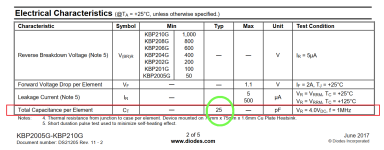
Looking at the datasheet for the bridge rectifier called out in the VRDN parts list, see attachment below, I note that the rectifier capacitance is 25pF x 4 diodes per bridge = 100 pF per bridge. Connecting three bridges to a single transformer secondary means the secondary sees 300pF of total diode capacitance. Fortunately, the "Starting Point" recommendation in the Quasimodo Design Note, suggests trying Cx = 10,000 pF (i.e. 10 nF ; i.e. 0.01 uF) across the secondary. The Design Note explains that Cx's purpose is to totally swamp out the rectifier capacitance, wiring capacitance, and transformer secondary self-capacitance. It replaces an unknown variable by a known constant. Since 10,000 pF is much greater than 300 pF, I would feel quite comfortable using the Starting Point value unmodified: Cx_with_3_VRDN = 10,000 pF. Or if you worry that the MOV's capacitance is much much much less than 10,000 pF: bodge-wire in a 4,700 pF capacitor in parallel with the MOV.
Then I'd just perform a plain old ordinary Quasimodo measurement on the transformer secondary, with Cx= 0.01 uF and with Cs = 0.15 uF and with Rs = 25 turn trimpot. Twirl the knob until the waveform is damped and the 2nd lumpity bumpity juuuuust disappears: done.
Attachments
Last edited:
Thank you, Mark, for a detailed answer with an elegant solution.
For Rs I plan to use the posted value of 44.2Ω since Santa Claus is not delivering my scope until December. 😳
Thanks again!
The MOV is 500 pF as mentioned so it certainly is much much less than 10,000 pF. I'll add the parallel 4700pF across the MOV as well.if you worry that the MOV's capacitance is much much much less than 10,000 pF: bodge-wire in a 4,700 pF capacitor in parallel with the MOV.
For Rs I plan to use the posted value of 44.2Ω since Santa Claus is not delivering my scope until December. 😳
Thanks again!
Applying that philosophy, I would completely remove all three snubbing components (Cacross, Rsnub, Cseries) from two of the three VRDN circuit boards
I do understand that there are three snubbing components, but the MOV does dual-duty as Cx and voltage clamping.
How safe are those two boards without the MOVs in place?
Thank you!
Parts arrived. Woo! Ordered a 1/2W part for Rs after reading the Qualsimodo_jig_revA.pdf document. Mouser was fresh out of bodge wire, though. 😉
- Home
- Amplifiers
- Power Supplies
- VRDN: bipolar regulator PCB for line level ckts: ±11V to ±20V @ 1.5A with "De-Noiser"