I read Hugh's (AKSA) recommendations about this amplifier . His recommendation is about the usage of the schematic in post #211.
I want to give a try to this if Ranchu can share the pcb in pdf or jpg format.
I want to give a try to this if Ranchu can share the pcb in pdf or jpg format.
Last edited:
Thimios, GEirin,
This is going around and around, and confusing everyone.
My original schematic was #158 for the other quasi thread on 22nd October from RANCHU32. We - both of us - worked on this schematic, Christian built and tested for sound quality, I did the LTSpice analysis.
To make this clear:
1. There was a nmos top and npn bottom.
2. The driver was omitted on the nmos; not required.
3. The 0.33R output stage resistor was inserted into the npn emitter to -ve rail.
4. The quasi Baxandall circuit was changed to 82R.
5. The bottom of the base resistor on the npn was taken to negative rail.
6. The nmos used a single 220R gate stopper; NO resistor taken to output node.
The correct, exact, specific schematic is, written by Ranchu32 himself, is #158 of this thread.
Hugh
Thanks AKSA ,so is there a pcb available according to this schematic?Thimios, GEirin,
This is going around and around, and confusing everyone.
My original schematic was #158 for the other quasi thread on 22nd October from RANCHU32. We - both of us - worked on this schematic, Christian built and tested for sound quality, I did the LTSpice analysis.
To make this clear:
1. There was a nmos top and npn bottom.
2. The driver was omitted on the nmos; not required.
3. The 0.33R output stage resistor was inserted into the npn emitter to -ve rail.
4. The quasi Baxandall circuit was changed to 82R.
5. The bottom of the base resistor on the npn was taken to negative rail.
6. The nmos used a single 220R gate stopper; NO resistor taken to output node.
The correct, exact, specific schematic is, written by Ranchu32 himself, is #158 of this thread.
Hugh
Hugh, my friend;
Good to see you back and still as brilliant as ever !
Would you suggest post#158 or Gelrins updated version with input differential ?
Good to see you back and still as brilliant as ever !
Would you suggest post#158 or Gelrins updated version with input differential ?
Weeeellllllll Thimios,
Christian did one, but may not be prepared to supply the artwork. I'm not sure; ask him.
I did something very similar, on Protel V1.12 .pcb, but I'm not prepared to offer it to the public domain. If this amp is superior to my present commercial offer, I would of course be using it. But until that time (and I have not heard my own pcb so I cannot compare to anything I've done in recent years, NAKSA/SAKSA etc) I will keep it to myself.
I would suggest that a quasi amp, while I know it's superior to most better than anything complementary around the traps, the world does not regard it as attractive at this time. The day harks back to the seventies in fact. The lower complementary PP amps are the favourites! I am surprised that so many people here are interested; perhaps people are changing their views, like Jaguar owners who are salivating at the forthcoming new straight six! OLD is NEW, huh?
Cheers,
Hugh
Sorry, I'll open another thread not to confuse.
This is another amplifier. My circuit is different from Ranchu.
Circuit diagram post 284.
1. Hybrid quasi output: a nmos top and npn bottom.
2. Drivers in each output transistors
3. TLP NPN
4. No miller cap in VAS
5. Shunt compensation before the VAS
6. Phase lead
Regards
This is another amplifier. My circuit is different from Ranchu.
Circuit diagram post 284.
1. Hybrid quasi output: a nmos top and npn bottom.
2. Drivers in each output transistors
3. TLP NPN
4. No miller cap in VAS
5. Shunt compensation before the VAS
6. Phase lead
Regards
Hi Balaboo,
You are still in NC? Welcome to you Sir, my Yankee mate....
I do not suggest the LTP version. The singleton offers more H2 and is far simpler, moreover does not have a S shaped gm curve. I like singleton; if the LTP is to be used I like to use CFPs for each device. THAT is very linear, particularly at higher output and current. Very nice to drive a quasi, in fact.
GEirin,
This goes on and on!
It seems to me that you have been given a lot of advice, and without a pcb you could build it very quickly on veroboard to try it out.
TLP is input stage, LTP?
I am no longer bothering to trawl through the thread, it's late, I need my ugly sleep.........
Ciao,
Hugh
Last edited:
Hugh, thank.
Circuit diagram post 284.
1. Hybrid quasi output: a nmos top and npn bottom.
2. Drivers in each output transistors
3. LTP NPN input
4. No miller cap in VAS
5. Shunt compensation before the VAS
6. Phase lead
Regards
Circuit diagram post 284.
1. Hybrid quasi output: a nmos top and npn bottom.
2. Drivers in each output transistors
3. LTP NPN input
4. No miller cap in VAS
5. Shunt compensation before the VAS
6. Phase lead
Regards
Hi GEirin,
I agree with you that it would be better to create another thread that is dedicated to discussing your interesting variants. While I welcome suggestions from members such as yourself on how to improve the circuit that is the subject of this thread, it seems that some of your comments are creating confusion amongst other would-be constructors about what is in fact the latest or definitive schematic, which I can once again confirm is the one from post #158, as also confirmed by Hugh.
All,
Unfortunately I don't have artwork to share because the layout matching #158 is yet to be completed. The built, tested amplifier I'm listening to uses boards adapted from a previous version, which I'm reluctant to share for all their obvious shortcomings. At some point when I finish the work I'll post the artwork here, and in the meantime, it would not be difficult for dedicated folk to wire this simple amp on veroboard or similar.
I've experimented with an LTP version of this design but dropped it in favour of the singleton input. I found through experimentation that a CFP VAS adds some refinement with this topology vs. the simple VAS (I've tried both) but I've never tried a CFP LTP, which I may attempt in the future to determine for myself whether the added complexity is warranted.
But to anyone who is even mildly interested, I say build the circuit at #158 and then see for yourself whether your modifications of preference improve or detract from the sound and post your findings here!
Hugh;
South Carolina (SC), son - land of the leader in domestic abuse cases.
I agree with the Singleton input, and prefer capacitor-coupling to the speaker.
South Carolina (SC), son - land of the leader in domestic abuse cases.
I agree with the Singleton input, and prefer capacitor-coupling to the speaker.
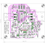
Hi Ranchu32 and AKSA,
Thimios talked me into it!😀
Here is a layout of your amplifier as per post # 158. I havent yet refined it and I thought its better to invite some comments before spending too much time into it. much of the PCB space is wasted which can be optimized later. So, its just a draft, as draft as it can be🙂.
reg
Prasi
edit: haven't read through the entire thread, but I understand that Q4 has to be mounted on o/p MOSFET + positive rail decoupling caps could be closer to mosfet pins.
Attachments
Last edited:
My Dear Prasi,
I have printed your wonderful graphic and I will examine it this evening in a warm room in front of TV...... thank you, it looks absolutely elegant.
I will give you my thoughts at the end of the weekend....
Thank you for your interest and great input in this very good amplifier from Ranchu.
Cheers,
Hugh
My Dear Prasi,
I have printed your wonderful graphic and I will examine it this evening in a warm room in front of TV...... thank you, it looks absolutely elegant.
I will give you my thoughts at the end of the weekend....
Thank you for your interest and great input in this very good amplifier from Ranchu.
Cheers,
Hugh
Hi Hugh,
Thanks a lot for your kind words. I am absolutely delighted that you are going offer comments on my layout. Thanks a lot again.
reg
Prasi
P.S. revised with R8, R9, C4 layout eliminating the jumper and to keep the trace lengths smaller around this area. You may have to take another print, sorry for that🙂.
Attachments
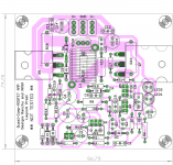
Hi, is this board layout (#294) designed to be placed vertically against a finned heatsink ?
Hi,
Yes, it can be placed vertically facing down so that o/p are as low as possible on the heat sink. heat transfer would be much better that way. but layout is not yet finalized🙂.
reg
Prasi
Hi Prasi,
Here are the points I noted. Please be aware these are just opinions; they are not hard and fast, just one person's views.
1. Most cap and resistor pads might be a little larger to permit removal for changing at a later time.... that is, for tinkling.
2. C1 is an electro. I believe in the input signal path this should be a film cap; typically a 1.5uF MKS with 5ps spacing. Electros do not sound good unless they have appreciable DC polarising voltage across them.
3. The Vbe multiplie you have used - Q4 - should be fitted on top of one of the output devices. If you do not link it with the output device, the amp will suffer thermal runaway. Locating this BD139 on the output device is best done with flying leads, OR, if you can do it, contiguous with the output device, using the same mounting bolt.
4. The Vbe multiplier will give too much tempco and when the amp gets hot the quiescent will drop far too much. You need to reduce this tempco. A good way is to insert a 3.3V zener, a 400mW zener, between the emitter Q4/VR2 and the connection of R10, C5, C8, R11, emitter of Q3 and base of Q5. The katod will point against the Vbe multiplier, and the anod to emitter of Q3. This means that Q4 will have around 5.5 - 3.3 = 2.2 volts across it, so R13 (2k2) will be replaced with 1k2. This will put the VR2 trimpot at around 600R and the entire bias generator will have the correct tempco.
5. Output device you describe Q8 should be redesignated Q6, and a text 'nmos' so you know which is mosfet and which is npn when you are building it! Lay out the amp as though an idiot is assembling it, then the chances of errors are reduced. Faults are very easy to develop if you don't describe and designate on the pcb.
6. Try to put Q6 (sic) and Q7 in the center of the pcb. Then you can mount the amp centrally onto a heatsink, attach the outputs with an M3 bolt and delete the four mounting holes, reducing the side of the pcb and making it installable with just two M3s.
7. D4 is a 1N4148. These are rated only to 100mA and the phase inverter might be developing up to 150mA with heavy load. Replace with a 1N4002.
8. C5 is a lag compensation cap and should be 33pF. Use silver mica, or styrene, nothing else.
9. C8 should be styrene or ceramic and should be increased to 68pF.
Prasi, you have quite a few minor changes, but the layout is good. If you make it a bit more compact, and set the outputs (and coil) centrally, it will be very attractive and easy to implement. These days the cost of double sided is almost as cheap as single sided, so you might like to explore this. Once you have it perfect, stare it foolishly for a week. You will undoubtedly find tweaks and fiddles which will turn a good board into a masterpiece.....
Ciao,
Hugh
.
Prasi, this is an very generous contribution, and I will be sure to look over your layout also 🙂
Thanks Prasi!
You are really fast!
Please keep this as single side,home etching friendly😉
Or, if you want,go for two versions.😀
Waiting for the final version.
You are really fast!
Please keep this as single side,home etching friendly😉
Or, if you want,go for two versions.😀
Waiting for the final version.
Last edited:
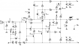
Thank you so much for the detailed suggestions. I have incorporated most of them (I think) and here are my comments on the same (in red)
Prasi
regardsHi Prasi,
Here are the points I noted. Please be aware these are just opinions; they are not hard and fast, just one person's views.
1. Most cap and resistor pads might be a little larger to permit removal for changing at a later time.... that is, for tinkling. Done
2. C1 is an electro. I believe in the input signal path this should be a film cap; typically a 1.5uF MKS with 5ps spacing. Electros do not sound good unless they have appreciable DC polarising voltage across them. Done
3. The Vbe multiplie you have used - Q4 - should be fitted on top of one of the output devices. If you do not link it with the output device, the amp will suffer thermal runaway. Locating this BD139 on the output device is best done with flying leads, OR, if you can do it, contiguous with the output device, using the same mounting bolt. Flying flying leads is what i could implement, as i am not so expert in lay-outing as some here.
4. The Vbe multiplier will give too much tempco and when the amp gets hot the quiescent will drop far too much. You need to reduce this tempco. A good way is to insert a 3.3V zener, a 400mW zener, between the emitter Q4/VR2 and the connection of R10, C5, C8, R11, emitter of Q3 and base of Q5. The katod will point against the Vbe multiplier, and the anod to emitter of Q3. This means that Q4 will have around 5.5 - 3.3 = 2.2 volts across it, so R13 (2k2) will be replaced with 1k2. This will put the VR2 trimpot at around 600R and the entire bias generator will have the correct tempco. Thank you for the revised values, incorporated the same. Schema also attached
5. Output device you describe Q8 should be redesignated Q6, and a text 'nmos' so you know which is mosfet and which is npn when you are building it! Lay out the amp as though an idiot is assembling it, then the chances of errors are reduced. Faults are very easy to develop if you don't describe and designate on the pcb. Done, designated o/p devices with names. 2SC5200N is a TO-3P device which is shown here but TO-264 version can also be used, only it will peak from under the PCB a bit. Yes, I know layout is not user friendly for assembling, but I have tried to keep important traces shorter and minimize the size.
6. Try to put Q6 (sic) and Q7 in the center of the pcb. Then you can mount the amp centrally onto a heatsink, attach the outputs with an M3 bolt and delete the four mounting holes, reducing the side of the pcb and making it installable with just two M3s. (o/p towards center)-Tried to do it as far as possible, but not nearly there, PCB size is now 75mmx75mm, I think it should be good enough for DIY. Its really a nice suggestion to mount the PCB on its o/p devices, people have to use some sort of spacer in between o/p device and PCB as there are solder pads on the o/p device.
7. D4 is a 1N4148. These are rated only to 100mA and the phase inverter might be developing up to 150mA with heavy load. Replace with a 1N4002.done.
8. C5 is a lag compensation cap and should be 33pF. Use silver mica, or styrene, nothing else. Thanks , incorporated, but those things are nearly impossible to get hold of in my part of the world.😱
9. C8 should be styrene or ceramic and should be increased to 68pF. done.
Prasi, you have quite a few minor changes, but the layout is good. If you make it a bit more compact, and set the outputs (and coil) centrally, it will be very attractive and easy to implement. These days the cost of double sided is almost as cheap as single sided, so you might like to explore this. Once you have it perfect, stare it foolishly for a week. You will undoubtedly find tweaks and fiddles which will turn a good board into a masterpiece.....thank you again for these particular suggestions, I intend to implement each and everyone of them( as a learning exercise).
Ciao,
Hugh
.
Prasi
Attachments

Last edited:
- Home
- Amplifiers
- Solid State
- Very simple quasi complimentary MOSFET amplifier