Hi GEirin,
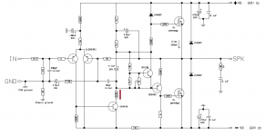
#239 is a good circuit sonically. BUT, there is considerable loss of rail efficiency because the mosfet in the quasi side requires about 5V Vgs for full drive, and this is well above the negative rail, which offers much more drive down to much lower output. Therefore this circuit will clip at around 6V off the negative rail, compared to a bipolar in the quasi role which will lose only about 2V off the negative rail.
The other, positive waveform is handled by the mosfet, which is driven from the bootstrap. You might expect this to deliver an early clip too, but in fact the bootstrap will kick above the positive rail, and the result is that the sound of the mosfet approaches within 2.5V of the positive rail. This approach is therefore delivering best clip. Using 36V rails and assuming no 'sag' on the rails, the maximum clip would be aroun 65Vpp (estimate from experience!) and this is very good from a hybrid circuit.
The other feature is the available of cheap bipolars (npn) and mosfets (nmos). The other gender devices are quite a bit more expensive, especially the pmos.
I also suggest that the baxandall 100R, 22nF and diode should be supported from the output node, not from the collector of the output npn. This is because the heavy current through the 0.33R collector current (not required actually) takes an additional (5 x 0.33) = 1.65V of the clip max on the negative half circuit. With a quasi you must design for maximum clip voltage; you have an inverting stage in there and it costs voltage!
Ciao,
Hugh
Hugh, thank you very much for your explanation and intention to help understand the circuit. I will study your instructions.
Ciao
Guillermo
Ciao
Guillermo
GEirin,
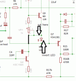
Disconnect anode of redled to VR1 and reconnect the redled to collector of T4.
Remove Q3, R4, R5 and D1 (zener) and replace with a 39k resistor.
Remove the bottom of R16B, reset it to 470R and connect to the negative rail.
Reset R17 to 82R.
That will ensure the quasi operates optimally.
Now, BUILD IT, then let us know how it sounds!
Ciao,
Hugh
Last edited:
GEirin,
Almost there!
I think I was wrong with the redled connection. My apologies......
Connect VR1 to Collector of Q4 and the Base of Q7.
Then the Redled anode is connected to emitter Q5 and katod to Collector of Q4/Base of Q7
some point as the bottom of VR1.
That's it.....
Hugh
Almost there!
I think I was wrong with the redled connection. My apologies......
Connect VR1 to Collector of Q4 and the Base of Q7.
Then the Redled anode is connected to emitter Q5 and katod to Collector of Q4/Base of Q7
some point as the bottom of VR1.
That's it.....
Hugh
Hi GEirin,
Not quite, but nearly there....
Anode of LED must be attached to emitter of Q5, and bottom of VR1 should connect to katod of LED, collector Q5 and base Q7. That completes it... enjoy the sound!
Hugh
Not quite, but nearly there....
Anode of LED must be attached to emitter of Q5, and bottom of VR1 should connect to katod of LED, collector Q5 and base Q7. That completes it... enjoy the sound!
Hugh
Attachments
Last edited:
Member
Joined 2009
Paid Member
If you really like the look of an LTP input you can configure it to behave like a Singleton and use the other device as a dc-servo controller - one of my earlier designs used such an approach with CFP drivers. It was one of my best sounding designs (until TGM8 that is).
http://www.diyaudio.com/forums/solid-state/167369-designing-tgm3-output-triples.html
As you can see, there are plenty of designs to choose. The real question is whether you want the challenge and reward of building something of your own design or build something already proven. Once you have that question answered you'll be off to the races!
Last edited:
One question: what is the function of collector R T Vas?
Thank
Do you mean the 820R?
Resistors are basically used to adjust current and voltage. In this case it is to adjust voltage. The preceding transistor has b-e connection to output so the base (of preceding TR) is around -700mV.
By putting resistor at the VAS collector, you lower the collector voltage to may be around -6V (from -700mV without the resistor).
The lower collector voltage might be needed if lower power dissipation is needed, or lower Vce is needed (without changing the gain of the stage).
Hi GEirin
Can you explain what your variation brings to be table over the original? Putting the nmos on top helps improve clipping symmetry, because the extra voltage headroom afforded by the bootstrap allows the mosfet to be driven closer to the rail. You loose quite a bit of headroom with your variant, and clipping on the -ve waveform will be distinctly asymmetric. Have a play in Spice and you will see what I mean.
But for all I know it might sound really wonderful and that is the compelling reason! Have you built and tested it yet?
Hello Ranchu32
greetings i am following this thread as i want to try this amplifier getting a
little confused as i dont know which is the correct tested schematic to
make this amplifier is it possible to point out the correct schematic
warm regards
Andrew
greetings i am following this thread as i want to try this amplifier getting a
little confused as i dont know which is the correct tested schematic to
make this amplifier is it possible to point out the correct schematic
warm regards
Andrew
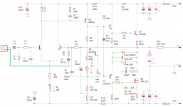
GEirin,
Go back to #231. That is the best circuit and I concur 100% with Ranchu's comments.
He did the work, he built and tested it sonically, and he carefully described and assessed it very well. Follow #231, do not change the mosfet and npn around; the mosfet should be at the top, the npn should be quasi.
Use the values used; no changes.
Eventually you stop talking about it and actually build it...... you NEVER know the results until you have the circuit working. This is a sublime amplifier; please BUILD IT AND CONFIRM WHAT OTHERS HAVE FOUND.
That is the benefit of DIYaudio........
Hugh
Hi Andrew
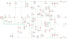
The schematic at post #158 is the current published circuit. You will immediately note the singleton input and associated biasing circuit, the latter necessary for reliable DC coupling of the speaker load. I believe the singleton sounds better with this design, for whatever reasons. In reality my latest version incorporates a few enhancements - some from Hugh and some of my own - that result in relatively minor improvements to the sound, but the overall sonic signature is intact.
There are two caveats to note:
- With this simple input biasing arrangement the offset can wander a little. During stress testing I have observed perhaps 200mV variation at the output, which should present no concern whatsoever. I did build a version with a DC servo consisting of a cheap opamp and a few passives that cured the problem completely but this is unnecessary in practice.
- The simple bias spreader tends to overcompensate. The cure is to install a red led in series with the bias spreader (and adjust the R's around the BJT control device as appropriate) or do as I do and mount the outputs to an oversized heatsink and bias it rich.
Christian
Should it be time to build one myself?
Christian,the schematic at post 158 is the right and working one?
Christian,the schematic at post 158 is the right and working one?
Hi all.
Thank you very much for your answers.
To build, I need to adapt the circuit a PCB that I have, NAP140 and a power supply of +36V - 0 -36V.
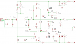
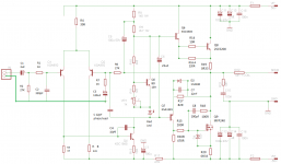
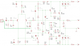
I have 2 circuits,
A) the Mosfet in positive rail.
B) the Mosfet in negative rail.
Thank you very much for your answers.
To build, I need to adapt the circuit a PCB that I have, NAP140 and a power supply of +36V - 0 -36V.
I have 2 circuits,
A) the Mosfet in positive rail.
B) the Mosfet in negative rail.
Attachments
Hello
greetings getting more confused which schematic to build post#258 is it good to try
warm regards
Andrew
greetings getting more confused which schematic to build post#258 is it good to try
warm regards
Andrew
- Home
- Amplifiers
- Solid State
- Very simple quasi complimentary MOSFET amplifier