Ilimzn,
Good input, thank you!
Since the bottom mosfet passes no gate current, the dissipation of Q7 will very little, since idle Vgs will be around 4.1V and at flat strap, at say 7A, the Vgs will increase about to 5V and while Q7 current increase, its Vce will decrease considerably as waveform passes to high negative potential.
Dissipation of Q7 is not that little - (4.1V/220)*(50V-4.2V) alowing for 100mV on 0R33 (negligible compared to other terms). That's about 850mW. But it is indeed correct that the dissipation does not change signifficantly. What does is the contribution on the 0R33 depending on the change of Vgs with temperature. That is, however, dependent on the heatsink temperature.
The temperature of Q7 should however be kept fairly constant.
That being said, I've looked into thermal stability with this design and it is almost impossible to simulate anything worthwhile with it because of model inaccuracy at relatively small currents (and 100-200mA is small for IRFP250).
You may well be right, however this has to be tested. The idea wit tying Q6 and Q7 thermakky almost as a rule results in overcompensation, as then Q7 Vbe change is (over) compensated and works only with the change of voltage on 0R33 versus change of Vgs. When Q7 is compensated, any change of voltage on 0R33 results from the Vgs change on the bottom MOSFET and since DC current can only flow through both MOSFETs (the NFB of the amp takes care that none of it goes tot he load by keeping the output DC zero), this automatically regulates both Vgs. However, there is a condition to be met. Increase in current of bottom MOSFET increases drop on 0R33 which 'pulls down' the Vbe multiplier. This should match the decrease of required Vgs of the top MOSFET for the same current. If there is a difference, then Q6 must reside on the heatsink to account for the rest, however, there is the factor 6-7 of multiplication of it's Vbe to get the proper Vgs. This may over or undercompensate, depending on small current behavior of the MOSFETs.
An alternative would be to use a Vgs multiplier and a diode in series, with the diode in thermal contact with Q7 (to take it's Vbe out of the equation). The Vgs multiplier MOSFET would then be in thermal contact with the heatsink, and as a bonus because it tracks Vgs almost directly, 0R33 could be reduced or possibly even removed completely.
Thanks Ilimzn,
Very good points, in particular the over compensation of a bipolar Vbe multiplier with a single, constant temp bipolar and a dynamically working source follower. I think the single Vbe mulltipler would be too steep, it is dropping around 4,8V for around 120mA quiescent and this is effectively 7.4 factors of the 0.65 pn junction voltage. I suspect that adding a LED at 2V in series with the Vbe multiplier, to reduce its Vce to around 3.8V, would be a good solution......
I did not address the degeneration issues of the 0.33R source resistor on the lower mosfet to rail. If output stage peaks at 7A, the drop across this resistor is 2.3V, and this must markedly increase the voltage across the gate resistor to rail, far more than I intimated in my previous email. This would improve quiescient stability but it would cost a lot of rail efficiency.
I also agree that only the empirical results are the best. I am gratified to hear that this is no longer a 'simple quasi'! The reason we move to more complexity is to improve performance - in this case, subjectively, since THD will be higher than a complementary design. Thank you for the catch diode from gate to rail, this was a find for me,
Cheers,
Hugh
Last edited:
I did not address the degeneration issues of the 0.33R source resistor on the lower mosfet to rail. If output stage peaks at 7A, the drop across this resistor is 2.3V, and this must markedly increase the voltage across the gate resistor to rail, far more than I intimated in my previous email. This would improve quiescient stability but it would cost a lot of rail efficiency.
Which is exactly why there is not one there 🙂
The ideal solution would be for delta the drop on the 0R33 in the CFP to match exactly the delta Vgs. Unfortunately, this happens only for far too large values of this resistor (it would have to be 1/S of the MOSFET and this is unlikely at low currents - 100..200mA - as S is quite low for those currents). Given a constant bias voltage (on what is now the Vbe multiplier) decrease of the Vgs with temperature on the lower MOSFET would then appear an increase of the voltage on the 0R33 resistor, which would pull down the gate of the upper MOSFET exactly by the same amount - marching the lower Vgs. This assumes Vbe of Q7 is compensated.
However, for realistic values of S of the MOSFET and realistic values of the 0R33 resistor, the resistor is too low in value so the Vbe multiplier has to do a part of the compensation. I think your idea with a relatively constant voltage drop element in series with the Vbe multiplier is a good one. One other one which I have seen is a TL431 with a string of diodes in the top part of it's voltage setting divider. Since it has a minimum voltage of 2.5V (and is temperature compensated), there are about 3 diode voltage drops to play with.
BTW interestingly no-one took up the schematic in post 171 🙂
Hi!
Is this design really "very simple"?
I am afraid not. It gets more and more complex. I think max. 6 active device should be used for this title.
Greets:
Tyimo
Its all relative, I suppose, and there are circuits here that are an order of magnitude more complex than this one, but on the other hand you could certainly remove a few components from this one and still have a working amplifier.
This is more complex than I had originally intended; however, I think the level of performance justifies those few extra parts.
I'm working on a small 3x4" single sided board that will be possible to etch at home and construct using low-cost through hole parts. So it should appeal to DIY builders I hope.
BTW interestingly no-one took up the schematic in post 171 🙂
I plan to come back to that one after I've laid out and built your other one 😉
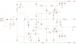
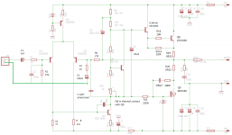
Getting close now I think...
I've repositioned the Vbe transistor to mount backside to the phase splitter, and put some room around these transistors as well as the VAS buffer to allow for a couple of small TO220 heatsinks. Might still require a small push/pull here and there for clearances.
Also replaced the diode at D2 with a 3.9V zener so that the upper MOSFET can make better use of the available gate drive.
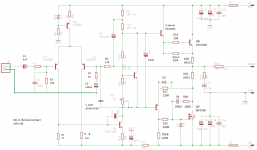
Attachments
Also replaced the diode at D2 with a 3.9V zener so that the upper MOSFET can make better use of the available gate drive.
No good I'm afraid, that will put the gate of the top MOSFET to permanent +rail less the zener voltage. It needs a series diode. In any case it's dubious as the extra swing comes at the expense of more asymmetric clipping. The zener increases only the positive swing.

Yes, it is a Sziklai amplifier. The final's input stage defines nomenclature. Therefore it is a P-channel Sz with an active load. It will sound sweet.
Yes, this works well. A Vbe to generate maybe 3.5V bias, and then a 4.7V zener to drop same, giving a bias generator of 8.2V using a complementary pair, about right for a mosfet output stage with 100mA quiescent. In this situation, you can ameliorate the tempco of the Vbe by inserting the diode into the Vbe between emitter and bottom output point just as Ranchu's schematic, simply substituting one (or two) diodes in place of his diode strapped transistor.
Hugh
Hugh
Last edited:
I spent a alot of time playing around with this topology and built something very close to your circuit, GEirin. If you decide to build it you will certainly not be disappointed. There is something almost magical about this nmos/npn quasi hybrid.
You can happily forgo the +ve side driver and R16A. Also, I now use a diode connected transistor as the Baxandall diode in my circuit.
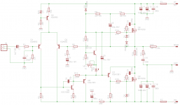
Personally I have abandoned the LTP in my own version as I feel the singleton input sounds better with this output stage (no idea why?). The current version I'm listening to is basically as per the schematic below, but with an elaborated bias spreader, different compensation schema, and several tweaked values:
http://www.diyaudio.com/forums/soli...imentary-mosfet-amplifier-16.html#post4194950
The only real disadvantage of the singleton is that the output offset tends to wander.... I've tried several methods, and I'm no fetishist when it comes to offset accuracy (+/- 200mV over the full temp range is AOK by me) but I *really* detest trimmers. So for that reason I also now use a simple DC servo, consisting of an inexpensive TL-072 and a few C's and R's, to bias the input. If you split the R at the output and put a small electro at the midpoint it cleans up the opamp muck without resort to regulated/filtered supplies. The result is great sound with few parts.
You can happily forgo the +ve side driver and R16A. Also, I now use a diode connected transistor as the Baxandall diode in my circuit.
Personally I have abandoned the LTP in my own version as I feel the singleton input sounds better with this output stage (no idea why?). The current version I'm listening to is basically as per the schematic below, but with an elaborated bias spreader, different compensation schema, and several tweaked values:
http://www.diyaudio.com/forums/soli...imentary-mosfet-amplifier-16.html#post4194950
The only real disadvantage of the singleton is that the output offset tends to wander.... I've tried several methods, and I'm no fetishist when it comes to offset accuracy (+/- 200mV over the full temp range is AOK by me) but I *really* detest trimmers. So for that reason I also now use a simple DC servo, consisting of an inexpensive TL-072 and a few C's and R's, to bias the input. If you split the R at the output and put a small electro at the midpoint it cleans up the opamp muck without resort to regulated/filtered supplies. The result is great sound with few parts.
Hi Hugh
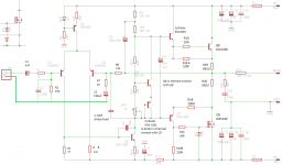
Take a look at the schematic and recall that this is the non-conventional "hybid" quasi circuit with a HEXFET on top and BJT CFP below. In this case I'd say about 4.8V total spread is about on the money, and would agree that 8.2V sounds right for a healthily biased complementary HEXFET stage.
A conventional bias spreader using a BJT control device overcompensates when used with MOSFET outputs. If you can find a red led that has a measured drop of about 1.7 - 1.8V and put it in series with a conventional Vbe multiplier taking up the rest of the Vdrop (BJT mounted atop one of the output devices) then it works pretty well.
I've also played around with more complex bias spreaders with this circuit, such as Figure 14.11(b) in Cordell's book, that allow must finer control over compensation ratios, but unless you want to to tune it to the nth degree its not really necessary. As long as you bias it rich and mount it to a large heatsink, the simple schema works well.
Yes, I realise that now.....
I'd done this some years back and found it very, very good. If the nmos is used at the bottom, you lose a huge amount of rail swing, so the npn you suggest improves this situation hugely.
I like the concept of setting the tempco 'rich'. Tuning a motorcycle engine, huh?
The hybrid design if usually used with a Brit amp (I think a Cambridge) in complementary; in your approach it's full on with quasi.
I very much like the quasi configuration because it throws a skew into the output waveform because of the differerent gm of each side; this creates more H2, and lots of people love this sound. But the technocrats think it's unacceptable because of the 'distortion', but this is good distortion, H2/H3/H4, a bit like good cholesterol....
Because of the prejudice to this approach you find that audiophiles, particularly the technical guys, avoid it.
Mind you, they like many of the chip amps, and they have quasi outputs!
Hugh
Hi Guys
The schemo in post-231 does not need the Bax diode, resistor or cap. The diode is added in BJT quasi amps to try to balance the impedance looking into the output stage from the VAS. In that case, there are two base-emitter junctions between the uppr drive line and the output but only one for the lower half of the circuit.
In the mos-quasi, you have one base-emitter junction plus a mosfet gate on the upper side but just a single BE on the bottom side.To balance the mos-quasi would require just the R and possibly a smaller cap to mimic the gate capacitance of a mosfet. Ideally, the balancing R would equal the gate-discharge R of the upper device. There are examples of this on the forum, one by Valery (username Vzaichenko).
Have fun
Last edited:

Geirin,
I strongly suggest you build this circuit from Ranchu: http://www.diyaudio.com/forums/soli...imentary-mosfet-amplifier-16.html#post4194950
It is a known quantity, he, Still4given, Tagstrip and a few others have built this amp and it sounds very, very good. The Quasi configuration is like any other; with careful, detailed design it can sound wonderful, and a hybrid approach seems to have sonic benefits. I believe it's because of the higher levels of second and fourth harmonic.
Ciao,
Hugh
- Home
- Amplifiers
- Solid State
- Very simple quasi complimentary MOSFET amplifier