Hi Valery,
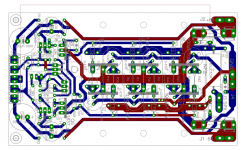
That looks pretty cool I'm not crazy about the SMD electrolytics. Any way to make them so the can use SMD and/or through hole.
That looks pretty cool I'm not crazy about the SMD electrolytics. Any way to make them so the can use SMD and/or through hole.
Hi Vallery ,this is the future!No more expensive parts.Peter, this is cool - I have recently come to the same kind of shape without seeing yours 😀

Hi Valery,
That looks pretty cool I'm not crazy about the SMD electrolytics. Any way to make them so the can use SMD and/or through hole.
Hi Terry,
Actually this is a good idea. In most cases there is some space for the holes (unless there is some dense parts load underneath), so it would be possible to make a universal design. I'll try to do it for the "Compact" series.
Thank you,
Valery
That would be great. I saw these in the other thread just didn't comment there yet. Most of us have a supply of through hole caps and it is much easier to solder them. I working n building up my supply of SMD resistors, diodes and ceramic chip caps.
Just do not use very small devices, we are no longer young nor robots😉Yep! 🙂
Valery
Cool board !!
Dual layer pcb gives a lot of advantages. I have made some measurements to compare the standard single layer OPS and dual layer OPS and there is slight measurable improvement in dual layer OPS. I run the V+ and V- rails very close (on top of each other), even better would be to run V+ and V- rails next to each other and putt GND track right above them, if the GND track would be a current return tor speaker than all the electromagnetic should cancel out.
The SMD emiter/source resistors --> I am using them in my PSU (5x 1R) in between the big caps, in case of short circuit they just pop like a fuse, saved my lab gear good few times, brilliant idea!!
Terry
I am comming back to lab at Tuesday and try to help a bit if I can with that tube.
I think the best way is to buy the brand new tubes the same brand so there will be no issues at all.
thimios
I have 33 years behind me but only 3 with soldering iron so eyes are still good, I can try some smd job in future anyway.
Regards
Peter
Attachments
I have 56 years behind me and about 40 with soldering iron so eyes are gone🙁Valery
Cool board !!
Dual layer pcb gives a lot of advantages. I have made some measurements to compare the standard single layer OPS and dual layer OPS and there is slight measurable improvement in dual layer OPS. I run the V+ and V- rails very close (on top of each other), even better would be to run V+ and V- rails next to each other and putt GND track right above them, if the GND track would be a current return tor speaker than all the electromagnetic should cancel out.
The SMD emiter/source resistors --> I am using them in my PSU (5x 1R) in between the big caps, in case of short circuit they just pop like a fuse, saved my lab gear good few times, brilliant idea!!
Terry
I am comming back to lab at Tuesday and try to help a bit if I can with that tube.
I think the best way is to buy the brand new tubes the same brand so there will be no issues at all.
thimios
I have 33 years behind me but only 3 with soldering iron so eyes are still good, I can try some smd job in future anyway.
Regards
Peter
Anything smaller than 1206 will be a problem.
I like your small output board.I wondering if i can etching this at home😕
Last edited:
This topology is VERY sensitive to impedance/gain of the first stage.
2sa/c to BCxxx , I had to change lag comp and reduce/tweak 2nd stage gain.
Vzaichenko also had to partition and calculate each stages gain.
I also notice you use no lag comp. I could not even get this topology to
work with BJT/FET without this.
Terry mentioned " where is the LTP" ? The tube is acting as one. An analogy
to the same amp with Jfets would be plate=source/grid=gate/cathode=drain.
On this thought, 220R + 220p across the plates would be the lag network.
This gave a perfect bode/phase margin with the Jfets @ 1.1ma Id.
Confirmed - without the lag , changing the Jfet model or degenerating it (gain change)
will make the amp unstable. The changing physics of the tube would be the same.
With the lag , nothing could create a "peak" beyond where there was sufficient margin (a sign
of instability). My lead and miller comp at VAS is also very similar to this one. (as are all my currents).
The ONLY reason this amp can even work is that the second stage is CCS based.
OS
Last edited:
Is this that you mean?This topology is VERY sensitive to impedance/gain of the first stage.
2sa/c to BCxxx , I had to change lag comp and reduce/tweak 2nd stage gain.
Vzaichenko also had to partition and calculate each stages gain.
I also notice you use no lag comp. I could not even get this topology to
work with BJT/FET without this.
Terry mentioned " where is the LTP" ? The tube is acting as one. An analogy
to the same amp with Jfets would be plate=source/grid=gate/cathode=drain.
On this thought, 220R + 220p across the plates would be the lag network.
This gave a perfect bode/phase margin with the Jfets @ 1.1ma Id.
OS
Attachments
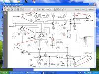
Is this that you mean?
Yup , my highly degenerated bjt's on the Kypton V are also a "further"
analogy to what the valve is doing in this setup.
The valve is different in that it changes a lot more than a solid
state device. temp/age/microphonics.
Jfet = another , but perfect - voltage controlled "valve".
I bet this design would sound identical with the proper Jfet.
C17 and C7 are also crucial (leads).
OS
Last edited:
Os, is this <<different>> listening because this want 500 mv only for full power(high gain)?Yup , my highly degenerated bjt's on the Kypton V are also a "further"
analogy to what the valve is doing in this setup.
The valve is different in that it changes a lot more than a solid
state device. temp/age/microphonics.
Jfet = another , but perfect - voltage controlled "valve".
I bet this design would sound identical with the proper Jfet.
C17 and C7 are also crucial (leads).
OS
Last edited:
Os, is this <<different>> listening because this want 500 mv only for full power(high gain)?
That is just R12/13 = Xgain. Close to 40X ? (27X slew ips)
My stability margins still were good raising my gain 10X.
Edit - I have two fully simulated amps like this (GLA/V).
GlA + jfets is identical , I matched borys's currents. Good amp 20ppm-20Kthd.
Should be the same with the valve. Oh , C17 = 6-10p (lead comp)
OS
Last edited:
Very close to real(28.6v/0.54=52).That is just R12/13 = Xgain. Close to 40X ? (27X slew ips)
My stability margins still were good raising my gain 10X.
Edit - I have two fully simulated amps like this (GLA/V).
GlA + jfets is identical , I matched borys's currents. Good amp 20ppm-20Kthd.
Should be the same with the valve.
OS
It is interesting to raise an IPS gain from 27X to 35X Just for a try.
Edit - I have two fully simulated amps like this (GLA/V).
GlA + jfets is identical , I matched borys's currents. Good amp 20ppm-20Kthd.
Should be the same with the valve. Oh , C17 = 6-10p (lead comp)
IPS madness😱
Last edited:
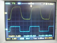
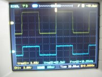
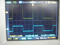
My first one with the 12au7 ran perfectly. Very stable offset and stable bias. This one with the 6n1p initially had that overshoot you saw in the scope shots. The offset is not solid. It drifts constantly especially when music is playing. With C7=33p and R3=120r, the top and bottom of the square wave look the same at 10vac but as you push the volume up the bottom of the square wave starts to flatten out and about 20vac you will start to see a slight overshoot developing. The top of the wave remains constant however. I have been running this with +-47v rails. Later today I will try running at higher rails and see if that improves things. This ips wouldn't even run at +-40v rails. I think the one with the 12au7 did. I have some ECC88 tubes coming. It will be interesting to see if those make a difference. Aside from all this, this ips sounds beautiful. If you didn't hook it up to a scope and DMM you would never suspect anything. It sounds very musical with solid bass clear mids and highs. As usual, I was too quick to build it so I missed out on the cool little led below the tube so I only get the natural glow from the plates. This was actually more fun to build than the first one because I got to play around with the values while trying to get it to work properly. The first one just played perfectly right off so it was off the bench quickly. Saying that, if I was planning to build one into a case it would be the 12au7 version because it seems more stable and I loved the sound.
Blessings, Terry
Blessings, Terry
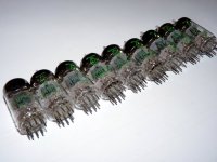
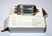
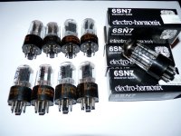
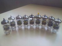
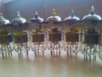
This afternoon as i tidy up some basement area i take a look at my electronic tube stock....and found some RT12AU7WA, 2 Sylvania Jan 6189, and some 6SN7 unit....
Attachments
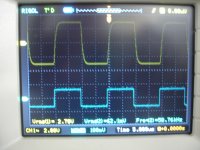
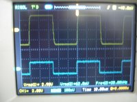
Now on the scope.
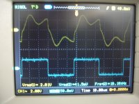
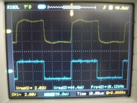
Picture No 6 6R//2.2uF DIRECT on amplifier out.
Picture No 7 6R//2.2uF AFTER LR filter out (direct on the load).
All pictures blue signal is input signal
yellow signal is out signal.
Valve =ECC82 RSD
Picture No 6 6R//2.2uF DIRECT on amplifier out.
Picture No 7 6R//2.2uF AFTER LR filter out (direct on the load).
All pictures blue signal is input signal
yellow signal is out signal.
Valve =ECC82 RSD
Attachments
Last edited:
platon
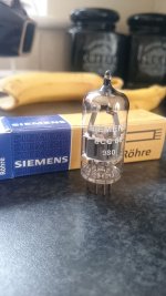
Nice army, I am not familiar with tube world a lot, tell me please if the Siemens I received today are any good ??
I am going to do some further development with ecc88 based amp and I need some decent tubes.
bimo
Nice work !! Can you explain me in simple words role of the R18=47kR resistor in NFB, it looks it is DC and AC coupled.
Thanks
Attachments
- Home
- Amplifiers
- Solid State
- Very Simple Hybrid Ampifier