another way of saying, gm reduction, since those resistors are in series with
the gm of the jfets....the series resistors decreases the jfet gm...
the gm of the jfets....the series resistors decreases the jfet gm...
output offsets pf +-100mV are acceptable since these
levels do not cause the speaker diaphragm to stray off dead center that much...
nor does it cause speaker coil burnouts..
levels do not cause the speaker diaphragm to stray off dead center that much...
nor does it cause speaker coil burnouts..
Increased input jfet Rs from 22 to 100ohm and now the amp starts to sound correct.
I will now reduce global feedback because with 22k FB resistor it sounds anemic.
Also will reduce TMC resistor from 2k2 to 1k8 to have better grip in the bass.
I will now reduce global feedback because with 22k FB resistor it sounds anemic.
Also will reduce TMC resistor from 2k2 to 1k8 to have better grip in the bass.
reduces the open loop gain and thus reduces the feedback. Makes for slightly increased stability margins.Increased input jfet Rs from 22 to 100ohm and now the amp starts to sound correct.
This could reduce the stability margins. go too far and you could go into full oscillation.I will now reduce global feedback because with 22k FB resistor it sounds anemic.
This sounds like guessing !Also will reduce TMC resistor from 2k2 to 1k8 to have better grip in the bass.
This sounds like guessing !
Not really, I already listened to several combinations.
Increasing the TMC resistor makes it less aggressive so sound looses snap.
Reducing the resistor increases snap but can also increase treble edge so 1k8 seems to be the best compromise right now.
now the amp sounds good but I believe I could do with a little more airiness so I will also try to reduce cdom from 120p to 100p or less.
As is (120p) and 100 ohm Rs it sims overdamped.
Attachments

After several experiences I settled for 27kohm feedback resistor, 100ohm source resistors in the LTP jfet, 220ohm resistors as emitter resistors in the LTP mirror, TMC 100, 1k8, 500.
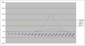
Gain is 30.5dB at 1khz in the Right channel that presents a perfect response curve flat to 100khz.
Sound is detailed and smooth... very good.
Now the Left channel is built exactly the same way but has a troubling anomaly.... The response is not linear and peaks at 100khz with 39dB.
As gain is controled by the feedback circuit I am wondering what component might be causing this.
Please verify the response curves ... hope someone can help me debug it...
Attachments
try checking the colours of the resistors for a wrong component.
Then measure each one, but this often gives low reading due to a parallel leakage of test current.
Then try checking all your installed capacitors.
And check the Zobel, for a failed resistor and/or capacitor.
There is a tool to check capacitor in circuit ESR. Useful in case there is a failed capacitor.
Thank you Andrew.
What is the tool you are referring to ?
During my initial experiments in the "wrong" amp, I experienced oscilations and the zobel resistor heated a lot.... will replace it along with the partnering cap.
I tryed to simulate this behaviour and the better aproximation is putting a large cap (2u) on the output... this produces a rise in gain near 100khz, but I do not have a cap during my bench measurements.
Another way to emulate the issue is using an inductive resistor for the feedback but in this case I need at least 0.1H to have this rise in gain at 100k, so it can not be the 27k resistor I have.
Do you believe a faulty transistor in the VAS or LTP might produce something like this ?
Replaced the zobel and now everything measures normally.
Thank you so much Andrew.
Now these amps sound big, fast detailed and sweet.
Thank you so much Andrew.
Now these amps sound big, fast detailed and sweet.
increase the ratings of the Zobel components.
Use a 200V or 250V rated MKT for the capacitor.
Use at least 4 by 10r 600mW metal oxide for the resistor. Metal film is OK, but metal oxide can tolerate more abuse.
Add on the second and third part of the Pi version of the Thiele Network.
10r+100nF for first shunt loop
5r||1uH for the series part
5r+100nF for the final shunt part across the amp's speaker terminals.
Each of the R are multiple 600mW to give sufficient power rating to cope with max power testing upto 20kHz sinewave and upto 10kHz squarewave.
A 10kHz square wave at 90% of clipping voltage will make the Zobel warm.
@ 50khz it will probably smoke.
using F-3dB = 1 / {2PiRC} you will find that a 100nF presents ~ 80ohms and passes ~0.5Apk when the 20kHz signal is at 40Vpk. That is a mighty big current.
Last edited:
Good job, it sounds like a nice amp. At least we didn't get bogged down discussing the merits of 20 different kinds of cascode...
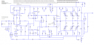
New improvements where done... please look at the new CCS in the IPS.
Droped the VAS active clamp.
Mosfet Bias now uses a LED for stiffness.
R18 does not have a bypass cap (It was responsible for a large offset)
All lateral mosfets have a Gate to Drain 15p capacitor that prevents oscillations.
Gate resistors have now different values for N and P devices.
IPS degeneration resistor where substantially increased.
Attachments
Important considerations:
IPS cascode transistors base voltage is obtained by a voltage divider that is referenced to the jfet IPS degeneration resistors so the cascode reference is an in-phase replica of the feedback devices collector signal.
IPS cascode transistors base voltage is obtained by a voltage divider that is referenced to the jfet IPS degeneration resistors so the cascode reference is an in-phase replica of the feedback devices collector signal.
Attachments
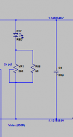
As I am using Lateral Mosfets that have a negative tempco after 150mA bias, thermal stability is assured so I do not need a Vbe multiplier to bias the OPS.
I am now using a resistor + LED arrangement. It is stiff and more linear than the typical bjt Vbe multiplier.
Must study this arrangement because in case of over current the LED will open and the OPS current will go sky high.....
I am now using a resistor + LED arrangement. It is stiff and more linear than the typical bjt Vbe multiplier.
Must study this arrangement because in case of over current the LED will open and the OPS current will go sky high.....
Attachments
- Status
- Not open for further replies.
- Home
- Amplifiers
- Solid State
- Very HQ power amplifier (Assemblage VII)