Mr Evil,
-Chris
I heard a preamp do that once. Amps make the same noise followed by BANG!Pffff. Some people have no sense of humour!
-Chris
Hi All,
I just discovered this thread by accident a few days ago. I have found it most informative and has taught me other things to consider about Vbe. The thread certainly has help me understand what I only knew prior as a divided preference to mounting or not the Vbe atop an output device or on heatsink beside. I wish I knew about this thread earlier as I had some specific Vbe qustions I posted in different thread regarding the very elements discussed in this thread. Oh well, what can I say? *hint you do not want to ask that question* 😉 lol lol lol lol lol lol
Anyway I like to ask what hopefully are a few simple questions (just assume all other elements are same for all these questions):
1) I found the idea of an all plastic TO-126, as opposed to those with metal about the hole at back, attractive for a Vbe. My reasoning, perhaps flawed, was I did not need to use any thermal insulation between the Vbe and heatsink thereby being better able to sense the temperature on the basis of overall less thermal resistance and lag. Make sense at all, even if theory? Is the mica/metal screw area are on back of a TO-126 better thermally resistance and lag wise? If has some merit depending on execution I like to her the thoughts.
2) I have also looked at a TO-220 based form factor to use as a Vbe. Part of reasoning is the larger surface area to be in contact thermally. As to insulated or not TO-220 mix in my thoughts of (1) above and offer your thoughts. I realize that for TO-220 the use of insulated may be a more varied consideration based on what was used and how thick the insulating coating is, as opposed to the TO-126 just being all plastic with no extra coating.
3) Are there any spec/electrical items and/or performance items that help one choose a ideal Vbe device?
4) Generally speaking how bad/indifferent is it to run a wire of say 4-6 inches from PCB to Vbe as opposed to Vbe directly mounted on PCB? Variants of this are do you twist the Vbe wires togther? Is it not much different to some PCB designs that run a longer set of traces to the Vbe so the Vbe can be placed in the more ideal position on the heatsink? I am sure there is a tradeoff of runing wire to Vbe in order to gain better chance at thermal tracking. So the essence here is in part the considerations to determine the best balance in such cases from the ideal of short trace and PCB mounted to the "ideal" location.
Regards,
John L. Males
Willowdale, Ontario
Canada
27 April 2006 15:45
27 April 2006 15:48 Opps a minior typo correction
Hi,
re long wires to a remote Vbe multiplier. If your multiplier has a bypass cap to carry the AC across the transistor then the long wires will have less effect. The multiplier is effectively a DC component but it does carry some signal. Twisted wires should not be a problem since any extra capacitance will be in parallel to the PCB mounted bypass cap already referred to. Parasitic capacitance (to ground or to circuit) is still a problem and hopefully some more knowledgable than us can help us out here.
Leach's slightly different set up using remote diodes is explained on his site, however both the clone and some other versions have reduced the number and/or location of the isolating resistors without apparent harm to the output quality.
My opinion is that the To126 would have less thermal inertia than To220 and result in a faster response. I see nothing wrong with supergluing a T092 to the output device or heatsink, it too should respond fairly quickly.
There are some isolated To220 devices that can be bolted straight on. I suspect there may be some isolated To126 devices as well. unfortunately all the manufacturers call them up with odd (different) type naming systems, so they are difficult to identify unless specified in the datasheet summary.
Hi Andrew,
Thanks for your reply.
Would I have to bypass each of E, B, and C or just one of these? I assume a 0.1uF would be the bypass cap value. Do you feel that it would be better not to twist the wires from PCB to Vbe?
I fully understand the difficulty in knowing if a TO-126 is "insulated" or not. What I did was go through all the transistor trays in the local parts store (each type of part is in own pull out try customers can take the parts they wish out of) to find out what part number of the TO-126 parts they had. That was more effective then searching net to find what I need only to find out the parts store did not carry that part, all plastic (insulated) or not. If you are familar with a MJE340 or MJE350 part in how looks there is a bit of metal on back about the mounting hole. What I happen to discover by accident was some TO-126 parts do not have the metal on the back, so it is like a TO-92 in that it is all plastic. As for the datasheets for the all plastic no metal at all TO-126's I did not see any indication on most of those datasheets related to the all plastic TO-126 part being an all plastic part with no metal. For all these all plastic TO-126 parts all the ones I looked up were all called TO-126, unlike the TO3P, of various different names manufactuers use for their TO-220 like insulated devices.
You raise a very good point about the thermal interia of a TO-220 form factor. It was on my mind. I did not mention size as factor as I was not sure the metal back of a TO-220 non-insulated part was less due to the all metal back when used with something like mica. Even if the TO-220 is insulated I wasl unsure if there is less thermal interia with the metal under the insulating coating of the TO-220. I was hoping, as you have, people would bring up any interia considerations. I will assume your TO-220 thermal interia being more covers both insulated and non-insulated versions.
I have seen in commercial and DIY projects that TO-92 devices have been used for Vbe. Some DIY people have been very creative in the TO-92 Vbe mounting. The classic mounting I have seem is flat side attached with silcone grease using the PCB mouning location at the heatsink. In my opinion the classic manner is poor thermal contact due to poor physical contact. I guess I am not comfortable a TO-92 form factor as I forsee various challenges to effect a good physical contact to the heatsink (skipping the technique of drilling a hole in heatsink) for a TO-92 Vbe. I will say the TO-92 form factor is very attractive for the reason you have suggested in terms of low thermal interia and no additional insulation required.
Regards,
John L. Males
Willowdale, Ontario
Canada
28 April 2006 05:10
I have been looking at the Vbe multiplier problem and came up with a solution that is in some ways the exact opposite of what D Self proposes. In his solution, he seems to encourage the use of high thermal mass coupling between the output devices and the Vbe multiplier (look at the response times and the amount of metalwork between the sensor and the output device(s)). I worked in analog instrumentation design for a long time, and one of the problemns I had to solve was thermocouple cold jnction compemsation. Using a similar approach on audio amps led me to use a small SMD transistor (BC870) placed in close proximity to one of the the output device collector pins. The thermal coupling between the devices is improved further by filling the immeadiate area around and between the output device collector lead and the sense transistor with heatsink compound. The distance between the two is about 3-4 mm.
Unfortunately, I could only attach the Vbe muliplier to one of the output devices, but nevertheless the technique works well - fast response (seconds) and on the 3 prototypes I built, and very good tracking, so Iq remained stable.
Hope this helps
rgds
Unfortunately, I could only attach the Vbe muliplier to one of the output devices, but nevertheless the technique works well - fast response (seconds) and on the 3 prototypes I built, and very good tracking, so Iq remained stable.
Hope this helps
rgds
By the way, I am using TO247 devices which are located on the underside of the PCB, along with the SMD Vbe sensor - all the other amp components are on the top side of the PCB - so thisis not a technique that is readily usable in desings where the output devices are mounted off board.
Hi ACR,
You can also mount silicon diodes between the legs of the outputs. If you were to add this to a heatsink mounted signal transistor you may find the results even better. I like to see a slightly negative temperature coefficient.
A hole drilled in the heatsink with a TO-92 case jammed in there generally works quite well. No problem with oscillation or noise pick up.
-Chris
Hi,
I have a reservation with To92 mounted in a hole drilled into the sink.
I suspect the curved surface is remote from the active junction area leading to high thermal resistance. The hole solution also ensures that the flat surface is disconnected from the heatsink.
I suspect that the flat surface is close to the active junction with just a thin layer of plastic encapsulation, thus reducing the thermal resistance and making reponse more direct.
Notice that I suspect a lot here, I do not know how these To92 devices are assembled.
The double flat package of an Eline could be even better if a copper clamping plate were used to ensure both sides of the Eline package are in thermal contact with the sink. It is the thinness of the Eline package (as well as higher Tj) that allows it to dissipate about twice the power of a To92 package and this implies that the junction is closer to the faces than the curved type.
Keypunch,
I would twist the three wires together.
The Vbe bypass cap goes from collector to emitter (by the shortest route possible) to connect the VAS to it's current source/sink. The routing of the multiplier resistors and the transistor are much less important than the direct path for the AC signal.
Hi Andrew,
Add to this that we are only talking about audio, not process control equipment. A small change in quiesent current level should not affect the audio performance that much. There are bigger fish to fry. You really only need to make sure your output stage doesn't turn into fancy looking wire bits. 😉
-Chris
You are probably correct here, but ... The curved side of the TO-92 package is in contact with the heatsink material. The thermal mass of the TO-92 is low whereas the thermal mass of the heatsink is normally high. The leads of a TO-92 case do not account for a low thermal resistance. I feel that the amount of thermal mistracking is small.I suspect the curved surface is remote from the active junction area leading to high thermal resistance. The hole solution also ensures that the flat surface is disconnected from the heatsink.
Add to this that we are only talking about audio, not process control equipment. A small change in quiesent current level should not affect the audio performance that much. There are bigger fish to fry. You really only need to make sure your output stage doesn't turn into fancy looking wire bits. 😉
-Chris
Andrew,
Thanks for your answers.
I also share your thoughts about Vbe TO-92 in a drilled hole in the heatsink. Your pondering the flat side being closer to junction makes some good reasoning for consideration.
ACR,
Couple things.
The questions I would have:
1)Do you mean BC870 or BC807. My hunch is latter.
2) Instead of the surface mount device solution you mentioned would you feel an all plastic (no metal on case outside) TO-126 is thermally more responsive than a TO-126 with metal on back with mica insulation?
3) Is the ideal location for sensing output driver temperature the Collector of a BiPolar Power output device?
4) What is the equavilant for a MOSFET power device to ideal temperature sensing point of the MOSFET power device?
5) Your preference device(s) for TO-126 case form factor?
6) Your preference device(s) for TO-92 case form factor.
Regards,
John L. Males
Willowdale, Ontario
Canada
28 April 2006 21:46
John,
1. Apologies - its a BC847C
2. With respect to the thermal response, difficult to say which is better. I have some experience in working with these issues and what seems to be intuitively the right often turns out to be completely wrong in practice. Only way is to try it the two approaches out.
3. Regarding which is the best place is dependent on your output topology. I use a straight output triple. The drivers and the output devices (5 per rail) are mounted on the same heatsink. The pre-drivers have their own heatsinks, but in most cases dissipate little real power. My first order approximation is that all three devices on one half of the output stage have a dVbe of -2mV. In practivce, because of the temp compensation scheme I have gone for, this turened out to be a pretty accurate assumption - Iq is quite stable over temperature (around 30mA delta from cold heatsink to very hot - uncomfortable to touch). Its also very fast with a response time of seconds.
Here is a picture of my solution before the heatsink compount has been put on. The output transistor is an MJL21193. The heatsink is 0.3c/Watt
rgds
Attachments
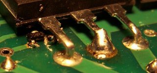
Vbe sensor placement
Interesting thread!
I am making a design with CFP output (one TO-220 driver and two TO-247 output devices, sharing 0.1R emitter resistors. All mounted on same heatsink.
Reading back here, it would be most effective to mount the VBE transistor close to on of the drivers, if possible direct on top of its metal flange?
Or would it be good to let the drivers and VBE transistor have their own common heatsink?
Hi,
I guess you mean one pair of drivers and two pair of output devices.
The two pair of output devices need an emitter resistor on each one i.e. four emitter resistors.
The CFP seems to need the Vbe multiplier temperature compensation mostly for the driver temperature, so it's better to have the Vbe transistor on a common sink with the two drivers.
Thank yoy Andrew....so there is no need for thermal contact between drivers and output devices?
The output devices are matched....do I need emitter resistors both on the emitters and the collectors of the output (CFP)?
There is base resistors valued 3R3 on each output device and the construction is the norwegian 12W class A from another thread.
What values would you recommend?
The output devices are matched....do I need emitter resistors both on the emitters and the collectors of the output (CFP)?
There is base resistors valued 3R3 on each output device and the construction is the norwegian 12W class A from another thread.
What values would you recommend?
Hi Scorpio
AndrewT is correct in that you only need the drivers and bias stabiliser joined (thermally but insulated) by a common heatsink which can be smaller than the output sink.
3.3 ohm base resistors - do you mean two per side? Even one per side would be low (you only need one) and would mean that the drivers have to turn on to drive ~200 mA before the outputs turned on.
That makes your current gain somewhat bimodal in your amp. Perhaps something like 33 ohms would be better - still bimodal, but the operating current is lower. I agree that you would need relatively low resistors, but you should aim to have the output transistors turned on a little (Class AB) to avoid crossover - unless, that is, you plan to operate in class A
cheers
John
for a to-92, i've seen a 2N3403 used as a bias transistor. it's a TO-92 transistor in an aluminum bracket, made for heat sink mounting, and the bracket surrounds the transistor package.
in the same amp, there is also a thermally sensitive resistor that decreases the audio input to the amp if the heatsink temp gets over 80C.
as far as TO-126 transistors go, a Harmon Kardon amp i'm repairing uses a 2SC3114 for a bias transistor.
also i noticed nobody has mentioned the japanese made "bias stacks" that consist of two series diodes in a heatsink mounted bracket. these are not adjustable as are bias transistor circuits, but i have seen them used on many older amps, primarily older sansuis and some early kenwoods (iirc)
Hi unclejed613,
Those "bias stacks" have been out of production for a long time now. They were normally used with a variable resistor in series to adjust bias current. I use a Vbe multiplier to replace them these days.
Almost any transistor can be used for the sense element. If it passes excess current you might want to use a low voltage 1/2 amp device or more. 2N3403 can be expensive compared to a 2N3904 in a hole. 😀 Carver and others used these.
The resistive element was usually a switch and could be used to do input mute, increase fan speed, or whatever. Temperature sensitive resistors require a circuit to interpret, that means cost and unlikely to be used in that manner.
-Chris
Hi all
the problem with bias transistor variation - going back to the start of this thread - is thatyou need to pick a bias stabiliser which has a Vbe which sits at about the same level as the Vbe of the driver/outputs. When multiplied by the resistor divider ratio, the overal bias current should be constant (ish).
IN one of the early posts (2005!) mention was made of different tracking performance with different transistors, and it was pointed out that the Vbe's of the different power transistors are different.
You can choose the bias stabiliser to give you different Vbe's by choosing the current rating, to a first order. For example, a BC237 type transistor may have a Vbe of 620 mV at 1 mA. If you run the VAS at 10 mA its Vbe will be around 680 mV. This won't give a good match to driver/outputs running at (say) 600 mV. The Vbe of a BD139 at 10 mA may be about 620 mV, giving good control for a pair of Bd139/BD140 and 2N3055/MJ2955 (don't laugh!) devices in a 50W amp.
But this didn't work for a pair of MJ15003/4's. To reduce the Vbe (on) I used a CFP for the bias stabiliser. BC237 running at a low current with BD140 passing most of the VAS current, and by varying the Rbe of the BD140 you can set the current in the BC237 to almost any value and therefore set the bias voltage (of the BC237) to almost any value you want (within limits). Self showed the circuit but I don't recall whether he explained the details.
If you want a bias stabiliser with lower Vbe at a given current, try using a TO220 stabiliser. 🙂
Hope this helps!
cheers
John
HI all.
In post 33, Mr. Evil said:
The best solution is to use MOSFETs. Choose them carefully and they will temeprature-compensate themselves!
Question: To use Vgs multiplier with BJT output?
Thanks
Guillermo.
In post 33, Mr. Evil said:
The best solution is to use MOSFETs. Choose them carefully and they will temeprature-compensate themselves!
Question: To use Vgs multiplier with BJT output?
Thanks
Guillermo.
I think he was referring to Lateral FETs, since his advice would be completely wrong for Vertical FETs.GEirin said:In post 33, Mr. Evil said:
The best solution is to use MOSFETs. Choose them carefully and they will temeprature-compensate themselves!
Question: To use Vgs multiplier with BJT output?
- Status
- Not open for further replies.
- Home
- Amplifiers
- Solid State
- Vbe Thermal Coupling Issue