Did you even read that application note? The device parameters were discussed in great detail. Data sheets for the Toshiba devices are available online; the designer need only use the Toshiba values in the equations.
Mr. Curl, you never answer my specific questions, you choose to bring up some other buzz word, redirect the topic, or take shots at me. Why not keep things technical? Did you actually try loading your circuit with the 1000 picofarads I suggested? You blasted me about the slew rate in the circuit I suggested, yet your original JC-2 didn’t slew as fast as mine. Not unless you selected only the highest gm devices, which you didn’t specify, only the matching.
Regarding your latest comment, 5 times the gm, 10 times the gm, it doesn't matter. I would think an expert would have a better understanding of that. Every device has a transfer function whether it be a tube, a bipolar transistor or a junction fet. These Toshiba parts have higher gain, so the id values on their curves are higher than for say an MPF102. That was what I stated. They still show the same square law transfer response, the rate of change is just higher. They show the same idss min/max range common to JFETs. They do not possess some magical properties only to be unlocked by the chosen few. They are high gain devices with a correspondingly high input capacitance. That’s it. Like any device, they require proper bias to function correctly, or better yet, optimally.
I admit my name is not known in the audio community like yours is, but I've been doing this for a long time as well and am not a rank amateur, or a tractor mechanic.
OK, everyone, listen up. J-fet's work best when running closest to their Idss. This is because the Gm is highest at Idss and above, and the most linear, as well.
The 60% figure would work IF the Gm was low and the design required the device to move from Iq to 2Iq or to 0 Iq. This happens with a single device or a differential pair. Think it through. Because the Gm always increases with current, then the optimum point can be moved from 50% to 60%, because you can drive slightly over Idss without any real problem.
This is the Siliconix story.
The Toshiba situation is different.
The Toshiba devices have MUCH more Gm and usually less Idss. Therefore, these devices would be unduly choked off, IF they had to meet the 60% rule. You can actually work to 1.5 times Idss (peak) or even more, BECAUSE you will not get into any real trouble with slightly forward biasing the gate, AND it will work more linearily, as you have more current to start with, AND you will use less percentage of the Iq to drive the second stage the same amount.
Now a short comparison of Gm for two devices:
J271 Siliconix Gm might be 10K at 10ma (best estimate) probably less, maybe 8K
2SJ74 Toshiba Gm would be 42K at 10 ma
Ratio 4.2:1 or 5:1
PS Don't screw up the circuit, please.
JC
Guys,
Perhaps all of you guys are right, maybe not, but please, leave the circuit as it was designed, Mr. Curl knows what he was doing at the time and still is.
My approach is:
The best way to learn electronics is practice, and in this case, accept and respect the designers point of view.
I'm also a designer, an engineer etc. etc. and learned through the years that there is more between heaven and earth.
Just my 2 Cents.
Keep it cool gents 😉
Best regards,
Audiofanatic 😉
Re: JC
Well, Tom clearly said that he was discussing a design that is sold as a kit on the 'net. Furthermore, he gave clear engineering reasons for his recommendations. One may disagree with that, and hopefully that would result in an *engineering* discussion, rather than one-liners like "trust me, I know best".
As much as we should all respect ANY designer and his work in this place, it is a very rare design that cannot be improved in one way or another. Tom gave some sound advice; I'm glad that finally Mr Curl in his last post gave also engineering arguments, finally. That's something that helps us all.
Jan.
Audiofanatic said:Guys,
Perhaps all of you guys are right, maybe not, but please, leave the circuit as it was designed, Mr. Curl knows what he was doing at the time and still is.
My approach is:
The best way to learn electronics is practice, and in this case, accept and respect the designers point of view.
I'm also a designer, an engineer etc. etc. and learned through the years that there is more between heaven and earth.
Just my 2 Cents.
Keep it cool gents 😉
Best regards,
Audiofanatic 😉
Well, Tom clearly said that he was discussing a design that is sold as a kit on the 'net. Furthermore, he gave clear engineering reasons for his recommendations. One may disagree with that, and hopefully that would result in an *engineering* discussion, rather than one-liners like "trust me, I know best".
As much as we should all respect ANY designer and his work in this place, it is a very rare design that cannot be improved in one way or another. Tom gave some sound advice; I'm glad that finally Mr Curl in his last post gave also engineering arguments, finally. That's something that helps us all.
Jan.
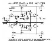
This same folded cascode configuration was used by Mr Borbely in his EB 604/410 /all- jfet Line Amp
(jfet second stage instead of BJT )
Rs =R5,R6, R8 , R9 = 100 R
R3 = 1k5
R=4 = 332R
R7+ P1 = range 47,5- 247,5R - depends on the Idss of the input jfets ( BL/V) set up the drain current of the input jfet at 2 mA !!!! ( each one )
If I understand correctly Mr Curl suggestions , those values aren't optimal , and this simple design could be improved ???
Attachments
It's been a while since I read those JFET papers, but if I recall correctly they were talking about the plain-Jane common Source, set the load resistor/bias current to half of rail for maximum voltage swing sort of thing. While this may be good advice for that one application, there are other approaches to amplification...such as the folded cascode, where you're depending on the cascode to handle the lion's share of the voltage amplification, not the input JFETs. Trying to make 60% of Idss into a one-size-fits-all solution isn't necessarily going to be the right answer in other circuit topologies.
Grey
Grey
Grey,
Agreed. This application note is a concise overview on JFET operation. It does not cover every application, but it does describe the device operation in good detail. I thought some DIY'ers might find it of use.
Agreed. This application note is a concise overview on JFET operation. It does not cover every application, but it does describe the device operation in good detail. I thought some DIY'ers might find it of use.
While I developed this exact topology,(Borbely's version) even down to active part count, in bipolar transistor form as early as 1968, it is DIFFERENT in optimum values than the JC-2 line stage. This is because the output follower BUFFERS the VAS stage, and it only has to create voltage swing, not supply output load current. In other words, the VAS stage doesn't have to do much, so it is easier to drive, and the input j-fets can be reduced in current. Then 2 ma or so is OK. You will find ALL Parasound power amps and preamps made this way for the last 15 years.
This is not the case when you are making a TRANSCONDUCTANCE amp and driving a difficult load. (potentially) This is when you need to beef-up the input stage so that it can effortlessly drive the VAS (and output) stage, in order to get 100ma or more peak current.
I used a cascoded form of this design to make the Grateful Dead line driver from the console in the audience to the stage. Now that was a challenge! Hundreds of feet of the worst wiring that you can imagine. No typical op amp could do the job, so they hired me to do it, after many years of absence, in the mid 80's. They were very happy with the result.
You might also note that Borbely's design doesn't even bother to turn off the output devices. They work at 100% and more than Idss. What a wild and crazy guy, and I told him that he should turn them down a little, maybe to 90% of Idss. He got very upset when I criticized him. 
My intended application for this circuit was as a preamplifier for my office system. I chose if for the simplicity, low cost, and small size. I have preamp out jacks so I can connect it to other amplifiers, but I use it as part of an integrated amplifier 95% of the time. I only have a single source input.
As such, I don't need to drive low impedance loads or long cable lengths. The amplifier circuit it drives has a 22K input resistor, so it is driving a light load. I bench tested it with heavier loads for reference.
In my application, and in most home applications, the preamplifier sees a relatively high load. Simplistically, the second stage gain will then be set by the feedback resistor in parallel with the load. With the parts I specified, the second stage voltage gain is approximately 120. With a 6 volt peak to peak output, the voltage to the second stage is 50 millivolts. The distortion of the input stage at that swing is largely independent of the input bias setting. I chose the resistor values I did for the second stage bias and for the open loop gain. Other values will certainly work. As Mr. Curl stated, running at idss will nearly double the transconductance and could provide 3 to 4 times the current drive for the second stage.
Interestingly, the hfe of the bipolar devices supplied with the parts kit start to roll off above 30 mA. The hfe is still 150 typically at 30 mA and probably higher as the part is warmer than 25 degrees C and hfe increases with temperature. It occurs with a 2N4401 also, but at a slightly higher current. The current required to drive the second stage depends on the output load impedance. With a low reactive component, the drive current is just the miller compensation capacitance. With a large reactive load, correspondingly larger drive current is required. The value of R11 limits the maximum current. Removing R11 allows additional current to be supplied to the load. If that describes your application, you would likely do well to heed the advice of Mr. Curl and crank it up.
My comments and opinions are based on the eBay kit, not as an upgrade to the JC-2. I’m not sure that was understood initially. I shared what I did and the results I had with the values I chose. I believe Mr. Curl has provided some valuable insight into operation in a harsher environment, and provided alternative values for your consideration.
Attachments

john curl said:It seems to me that you 1/2'd the slew rate and increased the input stage distortion 4 times, but I could be mistaken. Please don't second guess the original designer.
Actually the circuit in post #1 is sort of a FET version of the "current on demand" input stage like a bipolar "H-bridge" input. The concept of slew rate gets a little fuzzy, we make 'em with inputs running at 100uA that still slew at 3000V/us. You can tilt the input and get >Idss out with almost any value for the R. BTW the Hafler style complimentary circuits (long-tailed pairs with current sources to the rails) are not current on demand and have a slew rate in the classic sense. Last time I saw an ML2 schematic I though I remember seeing a FET current source floated between the input pairs, this would also eliminate that property (vs JC3).
Also 'back of the envelope' I don't see this circuit generating more than 8 or 10mV differential even driving 1000pF at 22V p-p at 20kHz. That keeps the thirds <110 dB (with ideal square law FETs). So the measuresd distortion must be all non-idealities, beta issues, etc. Of course this is with the values above, I don't know about the original. Running those TO-92 bipolars at 30mA ouch!
Scott, you still haven't contacted Dick Sequerra. Much would be resolved, if you would.
However, when it comes to this input circuit, I, at very first put a current source between the device pairs, but I soon realized that it was not necessary, and a resistor would do. I have used a resistor for the last 35 years, however Tom Colangelo modified the JC-3, to make the ML-2, (and they didn't have to pay me any royalties for my original design, then) and he added the current source between the device pairs.
I am just estimating distortion changes, based on changing the delta I / I ratio. This might be interesting and easy in a simulation.
The original design used HEATSINKED TO-5, 1-2A RCA devices, or TO-5 Solitron devices operating at peak beta.
The later JC-2 version started with RCA devices, then we experimented with 2N4401/4403 pairs and MPSA05-MPSA55 devices (I think). I am not sure what Mark settled on.
HOWEVER, ALL designs were filled with THERMAL EPOXY that acted as a heatsink.
The parts specified in the kit look OK for this operation, but they should also be heatsinked with TO-92 metal devices.
Scott, I am glad that you can see one of the advantages of comp J-fet operation not often noted or even completely possible with IC design. I pointed out this advantage to the audio press, at a 'Stereophile' seminar, about 10 years ago, using simplified diagrams and a viewer. Many of the audio press, John Atkinson for example, 'got it'.
john curl said:OK, everyone, listen up. J-fet's work best when running closest to their Idss. This is because the Gm is highest at Idss and above, and the most linear, as well.
The 60% figure would work IF the Gm was low and the design required the device to move from Iq to 2Iq or to 0 Iq. This happens with a single device or a differential pair. Think it through. Because the Gm always increases with current, then the optimum point can be moved from 50% to 60%, because you can drive slightly over Idss without any real problem.
This is the Siliconix story.
The Toshiba situation is different.
The Toshiba devices have MUCH more Gm and usually less Idss. Therefore, these devices would be unduly choked off, IF they had to meet the 60% rule. You can actually work to 1.5 times Idss (peak) or even more, BECAUSE you will not get into any real trouble with slightly forward biasing the gate, AND it will work more linearily, as you have more current to start with, AND you will use less percentage of the Iq to drive the second stage the same amount.
Now a short comparison of Gm for two devices:
J271 Siliconix Gm might be 10K at 10ma (best estimate) probably less, maybe 8K
2SJ74 Toshiba Gm would be 42K at 10 ma
Ratio 4.2:1 or 5:1
PS Don't screw up the circuit, please.
John,
Boy, I am having trouble following your statements... Interesting, while it seems to me that your rationale is mostly incorrect (or at best incomplete), your conclusions are correct! Kinda error correction mechanism 🙂
JFETs do not have any kind of "intrinsic" transconductance that Toshiba, Siliconix or Onsemi could magically adjust or target. JFETs have essentially two parameters: the device geometry (directly related to the Idss) and the threshold voltage Vt. The drain current is related (in saturation, where each and every JFET amp should run) to these parameters by the well known relationship:
Id=Idss*(1+Vgs/Vt)^2
The transconductance is defined as gm=d(Id)/d(Vgs) and therefore:
gm=2*Idss*(1+Vgs/Vt)/Vt
Gm is proportional with Idss, therefore is proportional to the device channel aspect ration W/L, which is a primary design parameter (given a certain silicon doping, which is mostly chosen based on the device breakdown requirements, so it's not an independent variable). Also, gm is inversely proportional with the device threshold voltage which is the Vgs at which Id is about zero (around the threshold the above equations do not apply, so Vt has to be "extrapolated").
Everything else like mobility degradation at high fields (which is essentially why transconductance is not linear with Vgs at high currents), fringing field effects, etc... are second order effects that can be mostly neglected in a low power discrete design.
And that's about it. If you are looking around Idss (that is, around Vgs=0) then gm0=2*Idss/Vt. At Vgs between Vt and 0 (and no, forward biasing the JFET is not a good idea, you are pushing your luck for some extra gm, that after all depends only linearly on Vgs) the transconductance is larger for devices with lower Vt.
The "magic" of the Toshiba devices gain is largely an urban myth. The Toshiba 2SK170/2SJ74 have three characteristics that makes them desirable (but not unreplaceable, I would say):
- They come pre-sorted in Idss classes. Rather than having a spec of Idss=6...50mA as the J271, the Toshiba devices are 2.6 ... 20mA sorted in three (G, BL, V) classes. Matching the Idss is certainly helping in matching the transconductances in a differential stage.
- Low threshold voltage of 0.15 ... 2V. That is, at the same Id, Toshiba devices have a larger transconductance.
- Low noise.
All of the above are related to a tight process control, most likely using ion implantation. Compare this with the 6...50mA and 1.5 ... 4.5V for J271, most likely a double diffused device. However, perhaps except for the noise performance, there's nothing that sorted and paralleled J271 can't do. Look at gm0 above! It's the Idss/Vt ratio that ultimately defines the transconductance at Vgs=0.
As a plus, as for their power MOSFET devices, Toshiba has matching (for transconductance, not for charges) N and P channel devices. While this is a nice feature, I wouldn't say it's absolutely required for good performance.
Why don't we have today more Toshiba like JFETs? Simple economics: they have a limited market and a semiconductor plant is definitely not a charity intended to bring happiness in the DIY communities. The same reason why the only transconductance matched MOSFET pair that I am aware of is the Toshiba 2SK1530/2SJ201.
I am getting my Gm numbers from the DATA SHEETS of both Siliconix and Toshiba. The rest is not very important.
syn08 said:
JFETs have essentially two parameters: the device geometry (directly related to the Idss) and the threshold voltage Vt.
The 2SK170, BF862, and J110 (I think) are all short channel devices, you can always tell from the excess gate current graph (John, the Linear Systems guys really ought to add that graph, the LSK170 is a little better than Toshiba). P devices don't do this due to the different mobility of the majority carriers. They all have similar high gm's at low currents. The BF862 has a little more 1/f noise but not too obtrusive probably due to whatever Philips did to get the Ciss/Crss so low.
Rode of Austrailia makes one of the lowest noise microphones around, using current SOT23 J305 FET's.
scott wurcer said:
The 2SK170, BF862, and J110 (I think) are all short channel devices
Yes, and so are Fairchild's PN4391, PN4392, PN4393, all sourced from Process 51. I have used some of these devices (namely PN4352) to achieve performances at par or better to 2SK170.
It is interesting to note the Idss/Vt ratio being almost constant which clearly shows that these devices have large process variations rather than being designed for certain "high gains".
Up and at 'em! You guys can do better than that! Start with process 88 Nat.Semi., or PS for (Siliconix). That is the MINIMUM that you MUST use and make a JC-2 type design with American parts. J110, as was used by me as input devices in Levinson JC-2 has NO compliment. Therefore it can only be used to make Bob Cordell's design, for example.
You guys can do better than that! Start with process 88 Nat.Semi., or PS for (Siliconix). That is the MINIMUM that you MUST use and make a JC-2 type design with American parts. J110, as was used by me as input devices in Levinson JC-2 has NO compliment. Therefore it can only be used to make Bob Cordell's design, for example.john curl said:Up and at 'em!
Well John, we may have here completely different views. Not having a marketing department to guide me, for the last six months I am banging my head against the piles of equipment I have here, trying to find a good technical reason why I should build a discrete preamp vs. using those new pieces of dirty sand called opa211, lm4562, lme49710, etc... I failed so far, but I am still trying. And no, listening to these things did not help.
Discrete solid state design has certain advantages. However, it is expensive, requires component matching, much of the time, and the parts are getting harder to get. Use IC's, if you can get away with it.
Mr. Curl
What was the idss of the input JFets on the ling stage you used on the original JC-2 circuit? I am now using JFets K170/BL & J74BL with idss 9.2~9.4ma and adjusted the Drain resistors from 100 Ohm to 150 Ohm and the Emitter resistors from 20 Ohm to 22 Ohm.
I am trying to do my JC-2 clone as close as possible to your original design.
🙂
- Home
- Source & Line
- Analog Line Level
- Variation on the JC-2 preamplifier