Ha! If you could do a sound comparison between your Badgers and the USSA that would be super interesting! The Badger is technically quite different, but sounds very good and is a well known reference to many diyAudio users.
p.s. I presently have Troels Faital 3WC-15 (built by the man himself) - they're very very good.
After getting some other projects out of the way (some by just not looking at them anymore), I am slowly preparing to build my USSA5. Two questions:
- Does it make sense to match the driver FETs (M3, M4) in any way? How?
- I will use the Smooth Like Buttah (SLB) power supplies. These will be great as long as the amp draws a constant current, i.e., as long as it operates in Class A. Is there anything I can do improve things when the amp goes into Class B? For instance, would it be a good idea to add more "real" capacitance after the SLB capacitance multiplier?
Hi Mbrennwa
Yes the mosfet drivers need to be matched to get best performance. The matching of fet driver is indicated in section 8.11 of the manual. Personally I am suite happy with version 5.1 using Sanken darlington bjt driver instead of mosfet driver. The latter do not need to be matched because Vbe is quite closed compared to VGS... also ordering Sanken bjt from big distributor will come from the same manufacturing lot.😉
If you use 1.2A bias output current you will never go out of class A up to 25Wrms (max power) into 8 ohms. As for 4 ohms, you possibly get about the same 25Wrms into 4 ohms in class A because of the square law effect of the mosfet with practically no degeneration (0.05 ohms). Regarding the latter I recently changed the source resistor from 0.05 to 0.01 ohms to increase the effect furthermore while still allow to easily measure the output bias current 😉. with the proper PSU you should get at least 40Wrms into 4 ohms but start to go in class B at more than 25Wrms. I recommend changing R15/16 to 0.01 ohms but the effect may be subtle...🙄
For the SLB I defer the question to other builders such as Meanie or maybe Vunce 😎
Good luck
Fab
Last edited:
Yes the mosfet drivers need to be matched to get best performance. The matching of fet driver is indicated in section 8.11 of the manual.
Hmm, I can't find anything about matching of the drivers in the manual. The only matching instructions are in Sec. 8.5.2.1, which explains to match hFE of Q1/Q2 and Q3/Q.
Section 8.11 is about checking if the driver transistors are genuine, not about matching them:
8.11 Driver transistors VGS verification (optional)
Verify Mosfet driver Vgs and YFS (transconductance) if you are worried that your Mosfet transistor may not be genuine.
8.11 continues with some instruction on how to determine transconductance, and to make verify it's within the datasheet specs.
How should M3 and M4 be matched?
...with the proper PSU you should get at least 40Wrms into 4 ohms but start to go in class B at more than 25Wrms.
Exactly my point. I want the amp to perform as good as possible even if/when it goes to Class B. That's why I am wondering about the best way to "expand" on the SLB cap multiplier.
I had the same thought, so on my SLB I changed the 220uF filter cap to 1,000uF. That's not a lot but there is also a 4,700uF cap on the amp board. However I have no scientific proof that this will improve things so I'm not suggesting anything.🙄
Perhaps you could ask on the SLB thread as I believe that X did increase the capacitance for an AB amp.
Perhaps you could ask on the SLB thread as I believe that X did increase the capacitance for an AB amp.
HiHmm, I can't find anything about matching of the drivers in the manual. The only matching instructions are in Sec. 8.5.2.1, which explains to match hFE of Q1/Q2 and Q3/Q.
Section 8.11 is about checking if the driver transistors are genuine, not about matching them:
8.11 Driver transistors VGS verification (optional)
Verify Mosfet driver Vgs and YFS (transconductance) if you are worried that your Mosfet transistor may not be genuine.
8.11 continues with some instruction on how to determine transconductance, and to make verify it's within the datasheet specs.
How should M3 and M4 be matched?
.
Ok I will clarify. Checking if N and P channels are genuine by measuring the ID compared to VGS will give you the data for matching. However, I had anticipated that one always buy advertised matched devices....🙄
For VGS tolerance you can use <=0.1V difference measured at different current values between 20ma to 50ma ID as a target. For transconductance It is the result of the previous data for matching so it is only used to check if you have the real part and not a fake.
My understanding of the SLB is that you can adjust it to deliver more current capability while increasing the voltage drop at output of the capacitance multiplier. If you target 2A-2.5A from the SLB for one channel then there should be no problem under max power into 4 ohms if the SLB is doing what it claims... however you need to take into account the voltage drop of the SLB for your PSU voltage.
Fab
Last edited:
For VGS tolerance you can use <=0.1V difference measured at different current values between 20ma to 50ma ID as a target.
Ok, thanks, that's clear now. My 2SK2013 / SJ313 parts all have Vgs values within 0.02 to 0.03 V, so all is good.
Next question: I will mount the driver and power FETs off board, using flying leads (10 cm long or so). I will mount the gate stopper resistors directly on the pins of the FETs, not on the PCB. What about the diodes D1/D3 and D2/D4? Should these also go to the FET pins? It might be nicer if I could keep them on the PCB, but that would mean the diodes will not connect to the gate directly, but to the gate stopper (i.e., between R17/R13 and R18/R14). Good or not?
You sure got matched devices if they are so close in VGS value😉
I do not like output device offboard 🙄 but I can understand that sometimes you have no choice for physical implementation. Gate resistor at mosfet pin is as you intend to do mandatory. For diodes located on board, to prevent destroying your precious mosfet matched drivers in case of diodes short circuit I would split the gate resistors in 2 : one on board (about 1/4 value) and the one on mosfet gate as 3/4 value.
But with diodes connected this way you do not have the same gate protection from over voltage. Lower voltage such as 9.1VDC may be more safe than actual 10VDC value.
Also, ensure you check for oscillation presence with that arrangement. A 10KHz square wave (<1VAC) into 8 ohms in parallel with Different cap Values may be a recommended test since I have not verified your arrangement. Overshoot should damped before one cycle. See example of figure 5 of manual.
And as a general rule for proper amplifier behaviour ensure you have very secured ground connections everywhere otherwise it will degrade substantially the performance and even lead to oscillation... The ground connections are the most important one.
Fab
Last edited:
Gate resistor at mosfet pin is as you intend to do mandatory. For diodes located on board, to prevent destroying your precious mosfet matched drivers in case of diodes short circuit I would split the gate resistors in 2 : one on board (about 1/4 value) and the one on mosfet gate as 3/4 value.
Ah, ok, now I realise that if the overvoltage protection kicks in (diodes short) at the gates of the output FETs, there should be some load resistance left for the drivers in order to avoid shorting the drivers.
I could do the split arrangement you suggested, or I could move the diodes off board onto the pins of the output FETs. The on-board way reduces the mess with "dead-bug construction", the off-board way would be better in terms of how the electronics are supposed to work. The on-board way would involve one (small) resistor at the FET pins vs. the off-board way with three (small) parts on the FET pins. I am leaning towards the off-board way (1 gates stopper + 2 diodes directly at the FET pins). What do you think?
“... I am leaning towards the off-board way (1 gates stopper + 2 diodes directly at the FET pins). What do you think?..”
Of course that will work but please check to ensure there is no small oscillation with long wires even with gate resistor directly to pin as I previously indicated.
Fab
Of course that will work but please check to ensure there is no small oscillation with long wires even with gate resistor directly to pin as I previously indicated.
Fab
Hi AnthonyA
+/-28VDC is fine but the maximum is 29VDC with no possible issue. The limitation is the J74 as per its datasheet.
If you build 3B ensure to have low IDSS for the jfet to have higher damping factor. You can expect to have DF of about 30 for 7ma IDSS and about 60 for 3ma IDSS. The DF is for 8 ohms load. For small size low efficiency or high efficiency speakers the lower DF sounds usually better. Note that 60 is still considered a low DF 😉
3B has a little bit darker sound compared to original version 3 or the version 3.1 which is under test in my listening room...
Fab
Last edited:
7.5 or 7 ma is about the same so you will get roughly 30 as DF which is most appropriate for many speakers.😉
There is a version 3 possible variant that I have not built yet: jfet input, mosfet driver (2sk2013/2Sj313) and bjt output. The mosfet driver would increase a bit the DF using the same jfet IDSS. But I wanted to get rid of the obsolete Audio mosfet driver... 🙄
It would be easy to change from 3B to the 3B.1 using mosfet drivers if you want to compare.
Fab
USSA-3.1
You need 2 sets for stereo...😉
I have been listening to the new USSA-3.1 with only 25 as DF and it really shines after long break-in and a couple of days listening ..🙂
Natural vocals, soundstage, instruments separation, dynamic sound and delicate nuances are impressive.
So do not let you fooled by DF value 😉
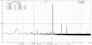
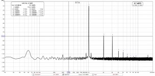
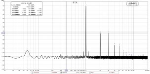
See THD profiles at 1W, 6W and 10W (all RMS) for 1k Hz under 8 ohms.
Fab
You need 2 sets for stereo...😉
I have been listening to the new USSA-3.1 with only 25 as DF and it really shines after long break-in and a couple of days listening ..🙂
Natural vocals, soundstage, instruments separation, dynamic sound and delicate nuances are impressive.
So do not let you fooled by DF value 😉
See THD profiles at 1W, 6W and 10W (all RMS) for 1k Hz under 8 ohms.
Fab
Attachments
Last edited:
Given all the talk about damping factor, I am trying to understand how the choice of certain transistor parts control the damping factors. How does that work, and why?
- Home
- Amplifiers
- Solid State
- USSA-5 Build with Review