Hi,
I finished first channel. When working on second channel, I messed up polarity, I accidentally connected VCC+ from PSU to VCC- AMP PCB and VCC- from PSU to VCC+ AMP PCB. C2, C4, C5 and C6 are gone. From C5 there was also some smoke going outside. It took about 10 seconds until I disconnected PSU. Is there any chances that I could destroy all transistors? J112, 557,547 and also TOSHIBA drivers were installed 🙁
Hi Amadeus00
I am sorry for you 😱
I suppose you mean C3 and not C2.
it is difficult to say if you damage transistors. I suggest that you measure them for possible short between their pins first. Bjt in diode mode of your multimeter should measure about 0.6 to 0.7VDC between b-c and b-e with polarity based on npn and pnp types. Jfet and mosfet should measure some resistance between pins.
Fab
Hi Thimios,
Do you have a link for the required SMD adapters for these?
Any sot23 to dip adapter will do the job.
Google it or look at ebay. 50 pieces will cost about 2euro.
Hello FAB,
So...as long as Point B to GND on the test circuit is 1.8v-2.8v @20mA the devices are genuine?
Hi tmas
That will not be enough. I recommend that you perform also section 8.11.2 where transconductance at various current (at least 20ma and 50ma) is checked.
Fab
Pay attention to pin out between SMD and throughole of J112 when mounting on USSA5 pcb.
Fab

I easily could have prevented this trouble... first real issue in 6 years...
However I tested a speaker and swapped the speaker wires on a live amp.
Normally no issue but the speaker + wire slipped from my hand and touched the shell of my (grounded) soldering station. My right channel went silent and I had a earth leakage trip.
Disassembled the right channel and measured
- power supply ok
- TP11-12 and 9-10 are 0mV
- TP7 psu + is 100mV (instead of 2,5V)
- TP8 psu - is 28mV
- Bias is zero
- I saw a white stripe from speaker + to the R27
Replace small transistors Q1-4 and J112’s first? Hope that’s all...
Could appreciate some help on repairing
Regards, Albert
Hi tmas
That will not be enough. I recommend that you perform also section 8.11.2 where transconductance at various current (at least 20ma and 50ma) is checked.
Fab
Hi fab,
I have been studying section and have a few questions:
1) Is the 15V V5 on the print a -15V supply? It is not labeled -15 on the schematic.
2) On Table 8.11.2.1. Are the various VGSN and VGSP measurements always taken from Points A,B to ground in the test circuit? Or the voltage at the actual MOSFET gate and source pins on the device itself?
3) What does the (10 Ohms) in the measurement table mean? I do not see a 10 Ohm resistor anywhere in the test circuit. Not sure what is being referred to here?
4) When "Matching" the devices. What measurement specifically is being targeted for matching? What tolerance is considered acceptable for the devices to be "Matched"
5) When "Matching" am I trying to match the +/- device in a pair or the pairs to each other in the R/L channels?
Hi AsandenI easily could have prevented this trouble... first real issue in 6 years...
However I tested a speaker and swapped the speaker wires on a live amp.
Normally no issue but the speaker + wire slipped from my hand and touched the shell of my (grounded) soldering station. My right channel went silent and I had a earth leakage trip.
Disassembled the right channel and measured
- power supply ok
- TP11-12 and 9-10 are 0mV
- TP7 psu + is 100mV (instead of 2,5V)
- TP8 psu - is 28mV
- Bias is zero
- I saw a white stripe from speaker + to the R27
Replace small transistors Q1-4 and J112’s first? Hope that’s all...
Could appreciate some help on repairing
Regards, Albert
Sorry to hear that. Hot swapping is always very risky and Murphy’s law always happen...🙄
If you had high voltage injected into the circuit then it is probably the worst thing that can happen.....then all small transistors are possibly gone and if not stressed too much anyway...so change them all.
While you have theses transistors removed you can measure the resistors to ensure they are not damaged too. Some of them are in parallel so you will measure the equivalent resistor value....
For the mosfet drivers and output Mosfet you can check if there are any short between pins. Diodes D1 to D4 may also be failed short and if so could have saved your output mosfet..😉
And R27 is gone for sure. It should be the first thing to check because it can be only that too 😉
C3 and c4 are rated only 16VDC so they may be damaged too.
Good luck
Fab
Last edited:
Hi tmasHi fab,
I have been studying section and have a few questions:
1) Is the 15V V5 on the print a -15V supply? It is not labeled -15 on the schematic.
2) On Table 8.11.2.1. Are the various VGSN and VGSP measurements always taken from Points A,B to ground in the test circuit? Or the voltage at the actual MOSFET gate and source pins on the device itself?
3) What does the (10 Ohms) in the measurement table mean? I do not see a 10 Ohm resistor anywhere in the test circuit. Not sure what is being referred to here?
4) When "Matching" the devices. What measurement specifically is being targeted for matching? What tolerance is considered acceptable for the devices to be "Matched"
5) When "Matching" am I trying to match the +/- device in a pair or the pairs to each other in the R/L channels?
1) V5 Polarity is properly shown so it is a negative polarity of course in relation to ground.
2) Points A,B to ground, voltage across gate resistor is negligible.
3) 10 ohms could read 22 ohms (mistake of the manual) but 10 ohms can be used too.
4) it is not intended for matching but to see if the device has a very good chance to be genuine instead of fake. The parameter checked is transconductance ( section 8.11.2.2) or Yfs in datasheet. You can use it for a “reasonable” matching too at a certain extend 😉
Fab
Last edited:
I easily could have prevented this trouble ... swapped the speaker wires on a live amp ... wire slipped from my hand and touched the shell of my (grounded) soldering station.
I highly recommend the use of "safety" connectors that have no exposed contacts. Example: https://spot.staubli.com/fileadmin/spot/22.2656_de.pdf
Look how is the original.....first photo and the good Chinese second photo.
Nikosokey,
Are you saying that the devices in the second photo are not genuine Toshiba parts, but function as well as the original Toshibas?
Tmas
If you do the measurements as per the test circuit for 20ma and 50ma and report the result I should able to tell you if the mosfet are genuine with a very high level of confidence.
Fab
If you do the measurements as per the test circuit for 20ma and 50ma and report the result I should able to tell you if the mosfet are genuine with a very high level of confidence.
Fab
Tmas
If you do the measurements as per the test circuit for 20ma and 50ma and report the result I should able to tell you if the mosfet are genuine with a very high level of confidence.
Fab
Fab,
Have not had a chance at this point. Just received the test devices over the weekend. Will report my findings as soon as I can get back on the bench.
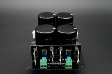
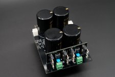
Nice PSU board you have with ideal bridge. It seems compact. Where did you source it?
You can continue to be optimistic😀
Fab
You can continue to be optimistic😀
Fab
I've designed them and they were produced by PCBWay. Some people learned new languages during lockdown, I decided to go with layouting and KiCAD 😀.
Hi Nfsgame
Good for you that you learn new things😉
I suppose that you already had the knowledge to do proper layout to minimize noise and crosstalk.🙂
Are the pcb with 2oz copper traces?
Do you plan to start a group buy?
How is your USSA-5 pcbs progressing?
Fab
Good for you that you learn new things😉
I suppose that you already had the knowledge to do proper layout to minimize noise and crosstalk.🙂
Are the pcb with 2oz copper traces?
Do you plan to start a group buy?
How is your USSA-5 pcbs progressing?
Fab
2oz copper on the boards, relevant traces are crosstalk-optimized (mainly between LT4320 and mosfets)
When the LT4320 daughterboards are working as they should I could upload the gerber files so that diy'ers who want to can send them to a PCB-house of their choice.
The "mainboards" could be used with TO-220 resistors on a heatsink or via an extra connector to small capacitancemultipliers (one positive, one negative). The capmx-boards could be mounted on the main-heatsink for example. Each amp-board will be connected via a molex-type connector.
My USSA5-boards are waiting for their powersupply. More progress on saturday.
- Home
- Amplifiers
- Solid State
- USSA-5 Build with Review