Speaker protection board power is taken from the amplifier: from GND pin on amplifier pcb and +Vcc on the psu pcb. I should have been more clear at the time but the cold-start graph with the 45V peak is without the speaker protection pcb in the circuit (which still requires repair).
The speaker protection pcb also tests for low amplifier (short-circuit) voltage as well as DC on the speaker outputs.
First 4700uF cap has been removed from the circuit and tests fine. Will do the second one now.
The speaker protection pcb also tests for low amplifier (short-circuit) voltage as well as DC on the speaker outputs.
First 4700uF cap has been removed from the circuit and tests fine. Will do the second one now.
Hi
GND pins on amplifier PCB are not used for connection to GND of speaker protection board. Both the PGND and GND pins on the amplifier pcb MUST go the main PSU GND. Check figure 21 of the manual. Otherwise you will have a floating input ground on the pcb. The speaker protection GND must be taken either at the GND speaker terminal of main PSU gnd.
Please confirm.
Fab
Both 4700uF caps were removed from the pcbs and both check ok.
In an effort to try to figure out where the errant voltage behaviour is sourced I removed the other speaker protection pcb from the amplifier and measured the 'good' amp channel and then swapped around the psu's and remeasured both amp channels again except with each others psu. Turns out that the cold startup overvoltage thing happens without the speaker protection board in the circuit on both channels, not just the problem channel, and both psu's give the same voltages on both channels...they are all behaving the same.
Re-tested the surviving speaker protection board and I think it may also be damaged because it is operating differently to when I put it in a week ago: opens at a much lower amp rail voltage than previously tested.
Fab, there is no Figure 21 in my manual (Rev 0.4.5) which was current at the time of the build. Are you able to email me through the (assumed) later version?
Acg,
Just a thought, do you have an inrush current limiter or “soft start” installed between your AC mains and trafo primaries?
Just a thought, do you have an inrush current limiter or “soft start” installed between your AC mains and trafo primaries?
I do Vunce.
The inter-pcb wiring arrangements are much clearer now that I have a more up-to-date manual from Fab, certainly not intuitive for my way of thinking. Hopefully changing one wire will help things...but it has to wait now...hopefully sometime this week.
The inter-pcb wiring arrangements are much clearer now that I have a more up-to-date manual from Fab, certainly not intuitive for my way of thinking. Hopefully changing one wire will help things...but it has to wait now...hopefully sometime this week.
Hi Amadeus
Good progress. So at this stage of the build have you tested the input stage?
I cannot see clearly the input transistors if they are touching together. There is a small advantage to have the input transistors to be thermally coupled for enhanced temperature control (DC offset, etc...). Take a look at other builds on the thread. This was a small improvement of the new pcb layout compared to the version 1 of the pcb.
Fab
Last edited:
Yes, I was able to adjust current in input stage, so far everything seems to be ok. I am using your manual step by step. I will try to couple input transistors, but they are already soldered and there is like 0,5mm gap between them.
When faced with the same issue, I simply cut a small metal spacer, slid it between the transistors, zip-tied the two together and used a drop of glue to make quite sure it couldn't move. It seemed a better option than straining the transitor legs.
Yes, I was able to adjust current in input stage, so far everything seems to be ok. I am using your manual step by step. I will try to couple input transistors, but they are already soldered and there is like 0,5mm gap between them.
Just put some heat shrink over the transistors.
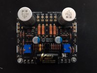
Front end testing.
Hi, I am not sure if that is an issue but when I adjusted 0,3Vdc between TP6 and V-, and then 0,3Vdc between TP5 and V+, I checked again voltage between TP6 and V-. But it was not 0,3V but dropped to 159mV. Is that OK? It seems that if I am going to try adjust same voltage between TP6 and V- and TP5 and V+, It won’t be possible.
Hi, I am not sure if that is an issue but when I adjusted 0,3Vdc between TP6 and V-, and then 0,3Vdc between TP5 and V+, I checked again voltage between TP6 and V-. But it was not 0,3V but dropped to 159mV. Is that OK? It seems that if I am going to try adjust same voltage between TP6 and V- and TP5 and V+, It won’t be possible.
Hi Amadeus
Are you at step 8.14 with M3/M4 installed?
If so, in some cases (depending on where you started from for the adjustment) there could be an extreme imbalance (DC offset) not being corrected by feedback. That is why you may need to put a low value resistor load at output to help balance ( refer to fig 18). You may need to redo the step starting by small steps, meaning small increment for P1 and then small increment for P2 and zeroing DC offset between each adjustment until you get to 0.3 VDC
Also verify that the diodes D1 to D4 are properly installed ans well oriented. You can lift up one diode for each path.
Fab
Last edited:
I have a critical question as i have i huge 1kw transformer, is it possible to run USSA5 using +/-20v?
Hi Thimios
Yes you can run with +/-20VDC without any change to the circuit. You simply will have less maximum power.
Fab
Yes you can run with +/-20VDC without any change to the circuit. You simply will have less maximum power.
Fab
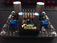
Front end testing Mk.II.
Hi FAB,
Thanks for reply. After I posted my issue yesterday, I decided to continue. I connected two VU meters to TP6 and V- and TP5 and V+ at the same time. By adjusting P1 and P2, I was able to get 300mV on both measured points. However, I needed to find balance because increasing/ decreasing of voltage was not linear or same for P1 and P2. Was also able to get 50 mV between TP4 and V- and TP2 and V+. After that, I measured OFFSET on output and it was 90mV, so I adjusted it to 0, however after 15 minutes it was 2,7mV and growing continuously (heatsinks were quite warm as well). There is one question: should I wait until heatsink reach stable temperature and then adjust offset or just adjust it immediately? Then I checked voltage between TP4 and V- and TP2 and V again, was same for both measured points at level of 48,7mV. VGSN was 0,914V and VGSP 1,509V. Back to your initial question, I was able to reach point 8.17. I checked diodes (types and polarity-should be OK). Just writing what I did in order to get approval or maybe some guidance. After you can confirm my results, I can do the math for Rv1a and Rv2a and then try to do another adjustment. Nevertheless, I will continue tomorrow since I am at work whole day today.
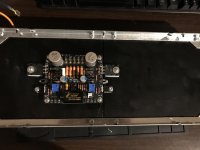
PS: You can see my PCB installation on heatsink. Not sure if this disproportionality of transistors layout might affect thermal characteristics and have some impact on overall results. I was considering also transformer and PSU position in my chassis, which is why I decided to install it that way.
One more thing. I was using my original PSU for all adjustment steps, only for 8.17 as intended in your manual. Not sure if it is good or bad …
Hi FAB,
Thanks for reply. After I posted my issue yesterday, I decided to continue. I connected two VU meters to TP6 and V- and TP5 and V+ at the same time. By adjusting P1 and P2, I was able to get 300mV on both measured points. However, I needed to find balance because increasing/ decreasing of voltage was not linear or same for P1 and P2. Was also able to get 50 mV between TP4 and V- and TP2 and V+. After that, I measured OFFSET on output and it was 90mV, so I adjusted it to 0, however after 15 minutes it was 2,7mV and growing continuously (heatsinks were quite warm as well). There is one question: should I wait until heatsink reach stable temperature and then adjust offset or just adjust it immediately? Then I checked voltage between TP4 and V- and TP2 and V again, was same for both measured points at level of 48,7mV. VGSN was 0,914V and VGSP 1,509V. Back to your initial question, I was able to reach point 8.17. I checked diodes (types and polarity-should be OK). Just writing what I did in order to get approval or maybe some guidance. After you can confirm my results, I can do the math for Rv1a and Rv2a and then try to do another adjustment. Nevertheless, I will continue tomorrow since I am at work whole day today.
PS: You can see my PCB installation on heatsink. Not sure if this disproportionality of transistors layout might affect thermal characteristics and have some impact on overall results. I was considering also transformer and PSU position in my chassis, which is why I decided to install it that way.
One more thing. I was using my original PSU for all adjustment steps, only for 8.17 as intended in your manual. Not sure if it is good or bad …
Attachments
- Home
- Amplifiers
- Solid State
- USSA-5 Build with Review