George , I also think that you should try opa860, in paper it seems better than AD844, the input impedance is 10 ohms , and the input stage quiescent current should be near 1.5mA , the equivalent to five AD844 stacked.
Connect Pin 1 to the -5V rail via a small value resistor, I use 10R, and the quiescent current becomes 12-13mA, no kidding. How many stacked AD844s would that be?
I have tried the OPA860 and even posted it in #615 (the only thing I would do is null the DC entirely and use no output cap).
It works.
Cheers, Joe
.
Joe, 12.7ma is the total quiescent current for the entire chip, but the buffer takes 5.8mA and it only remain 6.9ma for the OTA part , so if you divide this by 3, you get 2.3mA, in the simulador I get 1.5ma for 10 ohms of input impedance , but in reality the quiescent current in the input transistors of opa860 can get "maybe" up to 2.3ma.
I hope the picture helps in a better understanding. 🙂
I hope the picture helps in a better understanding. 🙂
Attachments
I would like to get to try the OPA861 one day, so Sergio you've measured the 861 quiescent at 2.3mA what is that compared to the 844 again?
And I was told by Jocko Homo once that Slew Rate was one of the more important specs to look for in an I/V stage. The 844 has 2000V/us where the 860/861 is only 900V/us.
Cheers George
And I was told by Jocko Homo once that Slew Rate was one of the more important specs to look for in an I/V stage. The 844 has 2000V/us where the 860/861 is only 900V/us.
Cheers George
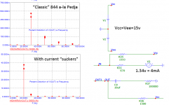
Biasing the 844 into deep class A should do some magic trick. At least in the simulator.
More than 20dB gain in the distortion department by sucking 8mA from input (-) and output (TZ) pins. The output resistor goes to Vcc as well as input resistor. Vcc=15v.
Then you might get some nasty DC offsets... so the cap should come on the input of the following stage, or whatever...
Yet... it might burn the 844 🙂 /*should be simmed with full internal schematics first to see all the transistors stay cool*/
Attachments
George, I did not measure the quiescent current, I just predict based on information on the datasheets and simulations. So I think that for the 844 the quiescent current at the input transistors may be between 250uA and 500uA, the opa840 between 1.5mA and 2.3mA, When a resistor of low value is connected between pin 1 and -V ,Joe uses 10ohms.
The slew rate of 2000v/us for the 844 is in closed loop , the slew rate of opa860 in close loop is 3500v/us , but in this case that is not important as the slew rate of the I/v converter are determinate by the filters capacitor at the TZ pin , and will be much slower, normally around 2v/us only.
But as Ken Newton said, the quality of the matched transistors inside the chips make a difference, and the 844 may have very well matched transistors for doing so well with such a low quiescent current.
Biasing the 844 into deep class A should do some magic trick. At least in the simulator.
More than 20dB gain in the distortion department by sucking 8mA from input (-) and output (TZ) pins. The output resistor goes to Vcc as well as input resistor. Vcc=15v.
Then you might get some nasty DC offsets... so the cap should come on the input of the following stage, or whatever...
Yet... it might burn the 844 🙂 /*should be simmed with full internal schematics first to see all the transistors stay cool*/
The current mirrors inside the 844 saturate at 10mA , injecting 8mA inside the chip is risky, using 5mA seems safer.
Do you have the full internal schematics?
no i don't... datasheet one should suffice to see the overheating thing, i guess...
Too bad we (huh, at least me) don't know where these TRIM pins go... we need to add some juice into AD's input stage.
My 844 model seems weird. huh... i don't remember whether i have modifiedd it or something...
Too bad we (huh, at least me) don't know where these TRIM pins go... we need to add some juice into AD's input stage.
My 844 model seems weird. huh... i don't remember whether i have modifiedd it or something...
Joe, 12.7ma is the total quiescent current
Quite correct, I stand corrected, and this is revealed by the OP861 (OTA only) that says about 7.3ma max (Figure 11), indicating the current feedback buffer in the 860 draws about 5.5mA.
So about 3.6mA (must tie Pin 1 to 4 via 10R) and that means that clearly the 844 is measured uA.
But look at my Technique 2. in Post #615, that would be my preferred option in any case, whether with either 844/680/681 because I know it works. I have done it many times with both 860 and 844. With 844 that 4R7 is way lower that "-" input Z and in the case of 680/681 still lower than 10 Ohm, but current headroom much better than 844. So all bases are covered with that technique.
It's not theory, it works!
You know, you can still get OPA660 on eBay - not good for manufacturing but OK for DIY. Genuine non-feedback buffer.
Cheers, Joe
.
You know said:Wonder what the pin 2 (E) input impedance is with the OPA660 (not stated)?
As the OPA861 is 10ohm to 13ohm in the data sheet, but it's not quoted for the 660.
Also the 660 has 3000V/us slew rate and 850mhz BW this is much better than the 861s 900V/us and 80mhz
Cheers George
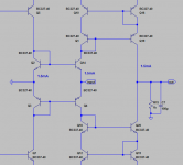
Some other I/V variations of common base thing from my sim files 🙂 Nothing new...
I/V Converters Galore
^^^ The performance seen on the HD plots is for ideal cases. Real world will kill it, unfortunately 🙁
I/V Converters Galore
^^^ The performance seen on the HD plots is for ideal cases. Real world will kill it, unfortunately 🙁
Wonder what the pin 2 (E) input impedance is with the OPA660 (not stated)?
As the OPA861 is 10ohm to 13ohm in the data sheet, but it's not quoted for the 660.
I suspect it will be similar.
Hi,
attached is the asc for Sergio´s idea in #610 (Btw: did You rename the AD844 and OPA861 file into .cir and .sub?)
Results:
A input Offset of ~80mV, hardly varying with different biasing currents.
Output offset can be trimmed, but sensitivity to R3´s value is high. Could probabely lead to thermal issues.
THD figures improve only slightly against the triple-AD844 circuit.
Harmonics decrease nicely with roughly -20dB/harmonic.
Noise figures increase considerably, especially the very high value of the buffered output is of concern.
Input impedance drops to ~5Ohms
Figures generally improve a bit with higher emitter resistor values (R1,2: 1k, R3: 1k01, R4: 1k2), but not so much that the mediocre results become good ones.
George, regarding #611, I´d suggest a different JFET. One with high Idss and high Vgs, as e.g. the 4391. This would allow for a considerably larger source resistor, thereby reducing noise and THD, increasing current stability and reducing the Idss variation within a charge of transistors (no, or less stringent matching).
jauu
Calvin
ps. forgot to attach the OPA861.asy
Attachments
Thanks very much Calvin , I will see if I can check your files again tomorrow.
Today I am filing a bit sick
Today I am filing a bit sick
I like the data on the OPA660 the 3000V/us slew rate, and the 850mhz band width, the only thing is what's it's input impedance on pin 2.
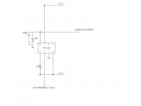
I have this idea to use it (attached) as this (without internal buffer) is the way the AD844/s are setup and it/they sounds magnificent with the +-1.2mA output of the PCM1704K and using the BUF03 as the output buffer. All comments welcome.
Cheers George
I have this idea to use it (attached) as this (without internal buffer) is the way the AD844/s are setup and it/they sounds magnificent with the +-1.2mA output of the PCM1704K and using the BUF03 as the output buffer. All comments welcome.
Cheers George
Attachments
Last edited:
Hi,
sorry Folks, the OPA861_Model sent in #618 needs a correction.
See Note 4 within the script if You open the model script with an editor.
The "ends xxx" command needs to be shifted to the very end of the script with LTspice.
Attached is the corrected file.
The file can also be found on the Yahoo-LTspice group
jauu
Calvin
Attachments
I have download from ltspice group, the xopamp_c.asy that I needed to run the Calvin file. And take a image for people that dont use the ltspice.
In this image are the fft from my proposal in #610, this simulate the pcm1704 at -6dbfs , as Calvin already said the harmonic distortion is not low, but the main component is 2º harmonic, the decrease in the harmonic distortion resemble the H.D. spectrum of tube circuits.
In this image are the fft from my proposal in #610, this simulate the pcm1704 at -6dbfs , as Calvin already said the harmonic distortion is not low, but the main component is 2º harmonic, the decrease in the harmonic distortion resemble the H.D. spectrum of tube circuits.
Attachments

I have download from ltspice group, the xopamp_c.asy that I needed to run the Calvin file. And take a image for people that dont use the ltspice.
In this image are the fft from my proposal in #610, this simulate the pcm1704 at -6dbfs , as Calvin already said the harmonic distortion is not low, but the main component is 2º harmonic, the decrease in the harmonic distortion resemble the H.D. spectrum of tube circuits.
The Other Calvin simulation.
This image are from four AD844 stacked, this simulate the pcm1704 at -6dbfs ,the main component of harmonic distortion is 3º harmonic, the pair harmonics are supressed by the complementar nature of the AD844.
Hi Sergio, why the big difference between the two on V(in)
Cheers George
... the only thing is what's it's input impedance on pin 2
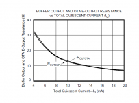
The input impedance is 7 ohms at 20ma of quiescent current, at 30ma the input impedance is probably lower than 5 ohms. The buffer of the opa660 is possible a good one also.
The tip from Joe, of using the opa660 is maybe even better than the opa861.
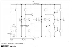
One interesting thing , is that the output impedance from the buffer is equal to the input impedance from the OTA. The quiescent current of the buffer is also regulated.
Attachments
Last edited:
Yes this OPA660 is making want to try it more and more.
The output buffer of the opa660 has only 1megohm input impedance and 15mA output current.
The output impedance of the 660 OTA pin 8 is 25kohm, I think it would rather like to see the fet input of the BUF03 being I think 5gigohm and it has 2ohm output impedance at 70mA.
Cheers George
The output buffer of the opa660 has only 1megohm input impedance and 15mA output current.
The output impedance of the 660 OTA pin 8 is 25kohm, I think it would rather like to see the fet input of the BUF03 being I think 5gigohm and it has 2ohm output impedance at 70mA.
Cheers George
- Home
- Source & Line
- Digital Line Level
- Using the AD844 as an I/V