
Yes, google.com suggests videos, but I am more comfortable studying texts, particularly when they are written structurally in a well planned way. I am one who finds good books an irreplaceable learning resource.
Since, I am almost ready making the first PCB, I am posting the files for evaluation and assessment.
Since, I am almost ready making the first PCB, I am posting the files for evaluation and assessment.
Attachments
Please "print" it or "export image" or show screen capture so it can display in the Forum window as a graphic image, otherwise you force us to install Kicad just to see it.
Also:agree +1000 with studying from well written books any day of the week, but Kicad being "new" , "open source" and "non commercial" will hardly lead to a printed book.
That said, there must be some kind of tutorial in PDF or HTML version which accounts as such, quite different from a "You Tube guy talking".
You might even print it on paper.
Here: https://docs.kicad.org/4.0/en/getting_started_in_kicad/getting_started_in_kicad.pdf
Here: https://xtronics.com/wiki/images/KiCad_Tutorial.pdf
bet there´s more out there, search even offered some in Spanish, because I am in Argentina.
Last edited:
Curious has anyone had experience with either pcb or librePCB? I tried kicad and pcb but was not liking either much. librePCB seemed to have more familiar interface to me, but I think very new and limited. Any other options for linux that are free for hobby?
I'm familiar with LibrePCB (although I haven't tried it yet) but not with an application named "pcb." Can you provide a link?
http://pcb.geda-project.org/ I found it when I searched in synaptic (the package manager in ubuntu) for pcb.
JMFahey said:Please "print" it or "export image" or show screen capture so it can display in the Forum window as a graphic image, otherwise you force us to install Kicad just to see it.
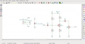
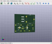
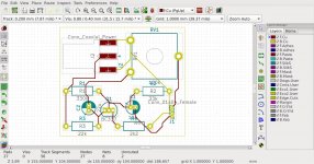
Here are three screenshots: (circuit diagram, PCB in the designer, PCB in the 3D viewer)
Attachments
Step by step we are getting closer.
Maaaayyyybeeee "connection error" warnings come from tracks reaching pads, but not being actually connected to them.
Zoom in suspect connections and check.
Some design packages are "polite" and once a track touches any part of a pad, "they are connected", others are very fussy and unless pad center and track end have exact same coordinates, with zero tolerance for differences, "they are not connected"
And even if, sometimes tracks can be disconnected from pads, for the purpose of rerouting them or connecting elsewhere, my point being that even "seeing" a track reach a pad, it does not mean they are vreally connected, hence zoom in and check.
Not sure it happens in Kicad which I don´t use, but hey, checking doesn´t hurt.
In some packages, you can click track and pad and ask to "join" or "connect".
PS: at some point increase track width to a more sensible value, I suggest 40 mil or 1 mm.
I tried to reconnect the "bad" connections following the advice from JMFahey although I was already aware. Since, the problem did not resolve itself, I think, the best thing is to remove the connectors and use vias instead. Vias allow wires to be soldered allowing a circuit to be built. At this point, my opinion is to continue instead of trying to solve this issue which might be caused by a bug or by something not properly set up in the footprint itself.
I will continue to do more exercises to improve my ability using KiCad.
EDIT:
Now, Eeschema is grumbling there is no connection at the removed connectors. This seems a hard bone to grind, and it will take its time. Having arrived at this point in my learning experience, I will not let myself be discouraged.
Last edited:
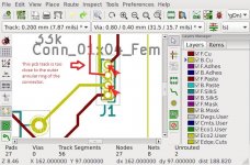
Finally, I am almost ready! I resolved the "no connection" error of J2. The idiot in me, did not realise it was as simple as using the 3D viewer to look carefully at connections. J2, for some weird reason unknown to me, created 5 pads, 3 on one side and 2 on the other. So, connecting the obvious pads always resulted into two unconnected pads.
To be truly ready, I need to block two Marker errors. I read there is a way to configure how, but I cannot find how and google seems to assume anything apart from what I mean it to search for. I am posting the marker errors for help to ignore these errors as what is actually overlapping are pad courtyards. Connectors are notorious for having crammed pins with crammed pads.
To be truly ready, I need to block two Marker errors. I read there is a way to configure how, but I cannot find how and google seems to assume anything apart from what I mean it to search for. I am posting the marker errors for help to ignore these errors as what is actually overlapping are pad courtyards. Connectors are notorious for having crammed pins with crammed pads.
Attachments
Last edited:
Teething pains 🙂
Yes, superimposed pads are hidden in plain sight.
Not sure what happened to you but I sometimes get that when I copy some component to be placed somewhere else , and by accident place one copy over the original.
Then everything there is duplicated but I see no difference.
Oh well.
Yes, superimposed pads are hidden in plain sight.
Not sure what happened to you but I sometimes get that when I copy some component to be placed somewhere else , and by accident place one copy over the original.
Then everything there is duplicated but I see no difference.
Oh well.
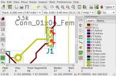
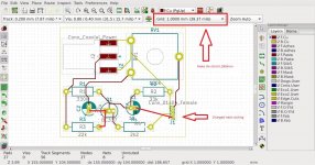
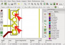
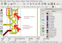
I think the DRC is indicating the pcb track to the left is too close to the annular ring of the connector, so its flagging it as a clearance issue.
The other error seems to stem from the schematic where Vcc is connected to Gnd via pins 2&3 of the connector J1.
See attached images.
Don't block these errors because in any case the pcb board manufacturer will run their own checks via the gerbers so the errors will get flagged anyway.
The other error seems to stem from the schematic where Vcc is connected to Gnd via pins 2&3 of the connector J1.
See attached images.
To be truly ready, I need to block two Marker errors
Don't block these errors because in any case the pcb board manufacturer will run their own checks via the gerbers so the errors will get flagged anyway.
Attachments
PWR_FLAG is a special purpose marker which tells KiCad a track is either power ground or a power rail. In the schematic there are no shorts, in fact, KiCad did not report any shorts of that type. The track almost touching the connector's pads should not be an issue, as KiCad's automatic track router passes tracks that way. Nevertheless, thanks for all those who took some of their time to help.
The solution seems to be to change the default net class's clearance to 0.15mm. Online it was suggested to use 0.199mm, but that, did not work, neither did 0.18mm. I had to go down to 0.15mm for the new setting to eliminate the error.
Since, I am new to PCB design, I am all ears to listen to criticism by others.
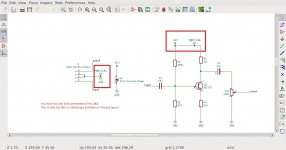
The problem is the PWR_FLAG is connected to Gnd at connector J1, so your power supply is shorted to ground, thats why DRC is flagging an error.
I gave an example in post #30 in how to run the pcb track to the connector to solve the clearance issues. For this type of pcb layout where you have plenty of space you don't need such small clearances, you should be able to use 0.25mm without any trouble. You don't have a clearance problem, it's a track routing layout problem.
Don't use the automatic track router, do it manually.............
Last edited:
PWR_FLAG behaves differently compared with other net lables. It only tells KiCad that a power track is driven. A power track can either be ground or a supply rail. You can confirm by searching in images.google.com using the keywords PWR_FLAG +"KiCad". There are several images showing PWR_FLAG being used on both power rails and ground.
KiCad's automatic track router passes tracks that way
Why are you using an automatic router?
Terrible choice, doubly so if you are trying to learn.
I imagined something of the kind when I saw your ultra narrow zigzagging tracks, and as close as possible to existing pads, where there was A TON of free space available.
+ 1000For this type of pcb layout where you have plenty of space you don't need such small clearances, you should be able to use 0.25mm without any trouble. You don't have a clearance problem, it's a track routing layout problem.
Don't use the automatic track router, do it manually.............
PS: Pilot Students do NOT use an Autopilot 😉
- Home
- Design & Build
- Software Tools
- Using KiCad.